• We’re currently investigating an issue related to the forum theme and styling that is impacting page layout and visual formatting. The problem has been identified, and we are actively working on a resolution. There is no impact to user data or functionality, this is strictly a front-end display issue. We’ll post an update once the fix has been deployed. Thanks for your patience while we get this sorted.

i7-3770K vs. i7-2600K: Temperature, Voltage, GHz and Power-Consumption Analysis

Page 2 - Seeking answers? Join the AnandTech community: where nearly half-a-million members share solutions and discuss the latest tech.
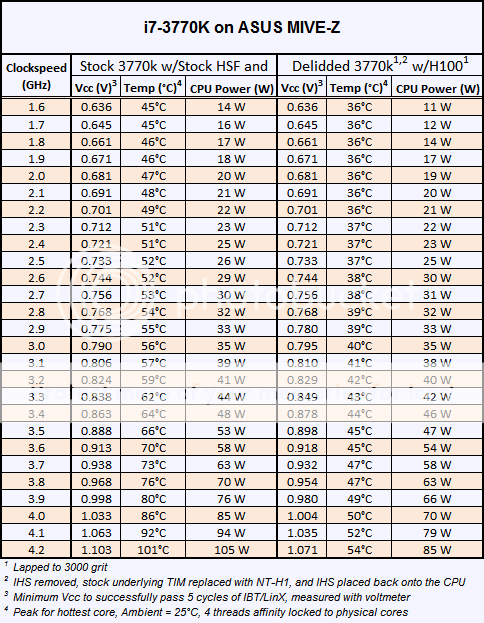
excellent posts IDC.

Wouldn't the surface area for static leakage increase since the finfet, increases the surface area around the drain? Also I am not sure how much the doping has changed in between 32nm and 22nm, which may be part of the static leakage non-increase.


I am surprised by the large drop in activation energy decrease ~30%. Granted the field-effect enhancement dropped significantly, thus the overall e^x value is approximately the same.

In future shrinks, it appears to me that the activation energy will drop even more and there won't be a large enough decrease in the field-effect enhancement to compensate thus there will be an increase in static power consumption in the 14nm shrink.

But then again I don't have an EE degree, just a biochemist who doesn't need to know much math so I am making assumptions for trends to occur to 14nm. It really does appear around 5-10nm will be a hard limit for CMOS shrinkage.

I would assume at that point static leakage will be a major issue and everything not in use will have to be voltage gated but they probably are nowadays anyway.

The "effective area" is difficult to relate to the inclusion of finfets because it is an "effective" or "equivalence" metric. It includes the BEOL (wires) as well as stuff leaking in and around the transistors combined with the substrate leakage.

The way to think of the "B" term is that it represents a value that comes from a weighted summation over all the leakage elements present in the IC, billions of them.

The same with the activation energy and the field-enhancement leakage, the values extracted from the data are just average values derived from the ensemble of billion of leakage points in the IC, each with their own activation energy and field enhancement effect, so what we are basically looking at is where the average values of the system has changed to.

The leakier components are going to dominate the parameters unless the weighting for them is very small.

I'm thinking the reduction in both activation barrier and field-effect leakage is a one-time offset that occurred because of the transition to finfet, meaning I'd expect Intel's 14nm to have essentially identical activation barrier (same dielectric materials) but higher field effect leakage (narrower dielectric spaces between the wires).
 
That was very interesting to read, I can only hope one day I'll reach a point in my studies where I can understand 1/4 of that.
 
😕 How so? Volts are volts and temps are temps.

All that delidding changes is the lowest temperature and lowest volts needed to be stable. Doesn't change the underlying device physics one iota.

A stock 3770k presumably would have a lower MHz advantage vs voltage due to higher temps. Would be interesting to have an unmodified 3770k added to the comparison.
 
A stock 3770k presumably would have a lower MHz advantage vs voltage due to higher temps. Would be interesting to have an unmodified 3770k added to the comparison.

You would also need a stock 2600k to compare it to, IDC didn't leave his 2600k stock either...
 
Just seeing the modded vs unmodded 3770K would be quite interesting with or without stock 2600K.
 
Just seeing the modded vs unmodded 3770K would be quite interesting with or without stock 2600K.

I have some data that was acquired prior to the modifications. What are you looking for? I will gladly pull together the graphical comparisons.
 
I have some data that was acquired prior to the modifications. What are you looking for? I will gladly pull together the graphical comparisons.

Clockspeed versus Peak Temperature

and

CPU Power Consumption

Differences are likely to be small but I'm curious what effect replacing the TIM (and lapping) had from stock.

Appreciate the effort you put into these posts, btw.
 
Clockspeed versus Peak Temperature

and

CPU Power Consumption

Differences are likely to be small but I'm curious what effect replacing the TIM (and lapping) had from stock.

Appreciate the effort you put into these posts, btw.

Sure I think I can pull those results together and make a nice comparative graph or table. Give me to this evening and I'll upload the table with the power numbers in it.

In the meantime if you haven't seen them yet I'll give you some links to some data that may answer those questions in a round-about manner. For instance checkout this thread and note the links in the OP to specific topics/posts that I felt merited extra mention (for example it turned out the CPU TIM itself isn't the problem, the gap is the problem).

Also checkout this post for data regarding CPU power and temperature for the 3770k, its buried in the OC'ing sticky so probably not many people saw it.

For the stock 3770k with stock HSF, this post has a data table in it that gives you max temperatures at min Vcc. I have the power data that goes with that table, just didn't include it in the table in that post. I'll pull them together and post it up later.
 
Wow, glad you pointed me to your gap test post. So if Intel had just made the IHS a tiny bit shorter... Are the IHS dimensions the same as with SB (assumption is yes)?

Thinking about it, tweaking the height of the IHS would probably be quite a big ask. Best to do that sort of thing on a socket change when lots of other validation needs to be done.
 
Last edited:
Is this more what you were looking for?

3770kStockvsDelidded.png


I doubt Intel would bother to invest the time and effort into optimizing/minimizing the CPU-to-IHS gap given that the CPU performs just fine when operated at spec in terms of clockspeed and voltage.

Its just us overclockers that find the gap to be very rate limiting because of the thermals.
 
Yes, that's the kind of info I was interested in. Thanks, Idontcare.

Since they are selling the K models for overclocking I don't think it's overly demanding from the consumer standpoint to push for better thermals. Whether that will get anywhere with Intel...
 
Was discussing water cooling solutions with a sales person from svc.com today. The rep was confident that some IB cpus were soldered, not TIM insulted between the heat spreader and die. I took his responses with a grain of salt. I highly doubt intel would change their manufacturing processes so drastically. He kept going on and on about SB being better.
 
Whenever I read an IDC post it's like getting hit in the head with the clue-by-four's evolved form, the baseball bat of knowledge.😱

That was a very enlightening read, IDC. Thank you.🙂
 
Is this more what you were looking for?

3770kStockvsDelidded.png


I doubt Intel would bother to invest the time and effort into optimizing/minimizing the CPU-to-IHS gap given that the CPU performs just fine when operated at spec in terms of clockspeed and voltage.

Its just us overclockers that find the gap to be very rate limiting because of the thermals.

Is there a comparison what kind of improvement the replacement of the TIM alone yields in terms of power consumption? Thanks.
 
Is there a comparison what kind of improvement the replacement of the TIM alone yields in terms of power consumption? Thanks.

I have that data too, but I need more info from you first so I can narrow down the data dump to something more specific to what you are looking for.

When you refer to the "TIM" are you speaking of the TIM that goes between the IHS and the HSF (aka HSF TIM)or the TIM that goes between the CPU silicon die and the underside of the IHS (aka CPU TIM)?

SchematicofCPUpackagecross-section.png
 
I meant the CPU TIM.

Ah, ok, in that case the result from replacing the CPU TIM was that it didn't actually change temperatures (and thus no change in power consumption) when replacing the CPU TIM.

All the benefits that come from delidding are entirely due to reducing the gap (the thickness of the CPU TIM). When I replaced the stock Intel CPU TIM with NT-H1 and intentionally kept the gap height the same my 3770k's temperatures actually went up a smidge, implying the stock Intel CPU TIM is actually slightly superior to that of NT-H1.

Checkout this post and this post.

DirecDiemounttemperaturesGraph.png


Getting rid of the thick CPU TIM (regardless what CPU TIM used) by reducing the gap height is what is key to reducing the temperatures (and thus power consumption) in these Ivy Bridge chips.

Getting rid of the IHS entirely and directly mounting the bare silicon die only marginally improves on the thermal conduction and heat transfer over that of getting rid of the gap itself.
 
Good to know, thanks!
One thing is not clear to me: If one removes the adhesive, thus reducing the gap, how will the IHS stay on the package and not fall off? The suction force of the CPU TIM may hold it a bit in place, but the contact are is small and the IHS is not exactly weightless. The pressure of the mounted HSF may help, but I would still be worried that after prolongued operation and movement of the computer case the IHS might slip downward, leading to a broken thermal interface.
 
Last edited:
@Boxleitnerb,

Once the cpu/IHS is in the socket with the hold down mechanism engaged, it's going nowhere. The hold down applies pressure on the sides (of the IHS). If you recall from IDC's delidding thread, you actually have to shift the IHS away from the socket a few mm before engaging the hold down, otherwise it shifts slightly when being engaged. Best to practice this BEFORE applying the TIM so you have some idea how much the offset is.
 
You're right, I forgot the hold down mechanism. Let's hope Intel fixes this gap thing with Haswell. I would delid it, but if I don't have to, all the better.
 
Back
Top