- Apr 27, 2000
- 23,159
- 13,254
- 136
Summit has been dethroned by A64FX. That's a heck of a linpack score, doncha think? And it did that without even using all of its nodes.

I think he was kidding.
A64FX is a pretty direct variation of the same microarchitecture Fujitsu has been iterating on since SPARC64 V, across three different instruction sets. (GS, SPARC, ARM)
Keller left AMD in 1999 when AMD canceled his new big K8a core based on Alpha EV8 (EV8 was super wide core with SMT4 and Keller was ex-Alpha engineer). But unfortunately AMD decided to just to evolve K7 core and implement memory controler into CPU like Alpha EV7 did.Then Keller was at beginning of PA semi, then bought by Apple, layed down first independent Apple uarch A6 (2xALU, OoO, 32-bit ARM) and A7 Cyclone (first 64-bit ARM core ever, 4xALU OoO pretty powerfull core, similar to Intel Haswell released in the same 2013, so yes, Apple had very competitive state of the art core like Intel since 2013) and Keller left Apple in 2012, one year before A7 release (but surely taped out) and left A8, A9 and A10 in development. He probably set goals for 6xALU monster A11 Monsoon family, including AMX and SVE. Then he decided to help AMD to return to the top and build super wide core with modern SIMD and SMT4 like EV8. Obviously he decided to create hybrid of A7 and Bulldozer first (Zen1) and then for next uarch to choose ARM ISA, super wide 6xALU+SVE/AMX core like in Apple.... and finally to implement the main feature of revolutionary EV8, the SMT4. But AMD staff was scared by parameters he has chosen for K12, they thought he is risking already a lot by deciding that Zen1 to be 4xALU (remember in 2012 there was no 4xALU on market, Haswell and Apple A7 came 2013). K12 spec was sci-fi like original K8a before cancelation. So later on K12 was cut down to 4xALU and SVE and later on sold to Fujitsu. Zen3 is a x86 version of K12 lite, so probably still 4xALU but powerfull FPUs similar to A64FX (no surprise, it has same roots, also some Zen3 leak mentioned 50% IPC jump in FPU load, confirming that). Since Fujitsu A64FX doesn't have SMT4, it looks like SMT4 was cut down from Zen3 as well. In Intel Keller is responsible for chiplet design of Alder Lake (8 big Golden Cove cores and 8-small Gracemont cores active out of 16-core Gracemont chiplet, fully 16-core capable chiplets will be used in Snow Ridge server CPU platform). So yes, Apples 6xALU core family, SVE, AMX, Fujitsu A64FX and Zen3/Zen4, chiplet Alder Lake are all Jim Keller's babys maybe.
Keller left AMD in 1999 when AMD canceled his new big K8a core based on Alpha EV8 (EV8 was super wide core with SMT4 and Keller was ex-Alpha engineer). But unfortunately AMD decided to just to evolve K7 core and implement memory controler into CPU like Alpha EV7 did.Then Keller was at beginning of PA semi, then bought by Apple, layed down first independent Apple uarch A6 (2xALU, OoO, 32-bit ARM) and A7 Cyclone (first 64-bit ARM core ever, 4xALU OoO pretty powerfull core, similar to Intel Haswell released in the same 2013, so yes, Apple had very competitive state of the art core like Intel since 2013) and Keller left Apple in 2012, one year before A7 release (but surely taped out) and left A8, A9 and A10 in development. He probably set goals for 6xALU monster A11 Monsoon family, including AMX and SVE. Then he decided to help AMD to return to the top and build super wide core with modern SIMD and SMT4 like EV8. Obviously he decided to create hybrid of A7 and Bulldozer first (Zen1) and then for next uarch to choose ARM ISA, super wide 6xALU+SVE/AMX core like in Apple.... and finally to implement the main feature of revolutionary EV8, the SMT4. But AMD staff was scared by parameters he has chosen for K12, they thought he is risking already a lot by deciding that Zen1 to be 4xALU (remember in 2012 there was no 4xALU on market, Haswell and Apple A7 came 2013). K12 spec was sci-fi like original K8a before cancelation. So later on K12 was cut down to 4xALU and SVE and later on sold to Fujitsu. Zen3 is a x86 version of K12 lite, so probably still 4xALU but powerfull FPUs similar to A64FX (no surprise, it has same roots, also some Zen3 leak mentioned 50% IPC jump in FPU load, confirming that). Since Fujitsu A64FX doesn't have SMT4, it looks like SMT4 was cut down from Zen3 as well. In Intel Keller is responsible for chiplet design of Alder Lake (8 big Golden Cove cores and 8-small Gracemont cores active out of 16-core Gracemont chiplet, fully 16-core capable chiplets will be used in Snow Ridge server CPU platform). So yes, Apples 6xALU core family, SVE, AMX, Fujitsu A64FX and Zen3/Zen4, chiplet Alder Lake are all Jim Keller's babys maybe.
Keller left AMD in 1999 when AMD canceled his new big K8a core based on Alpha EV8 (EV8 was super wide core with SMT4 and Keller was ex-Alpha engineer). But unfortunately AMD decided to just to evolve K7 core and implement memory controler into CPU like Alpha EV7 did.Then Keller was at beginning of PA semi, then bought by Apple, layed down first independent Apple uarch A6 (2xALU, OoO, 32-bit ARM) and A7 Cyclone (first 64-bit ARM core ever, 4xALU OoO pretty powerfull core, similar to Intel Haswell released in the same 2013, so yes, Apple had very competitive state of the art core like Intel since 2013) and Keller left Apple in 2012, one year before A7 release (but surely taped out) and left A8, A9 and A10 in development. He probably set goals for 6xALU monster A11 Monsoon family, including AMX and SVE. Then he decided to help AMD to return to the top and build super wide core with modern SIMD and SMT4 like EV8. Obviously he decided to create hybrid of A7 and Bulldozer first (Zen1) and then for next uarch to choose ARM ISA, super wide 6xALU+SVE/AMX core like in Apple.... and finally to implement the main feature of revolutionary EV8, the SMT4. But AMD staff was scared by parameters he has chosen for K12, they thought he is risking already a lot by deciding that Zen1 to be 4xALU (remember in 2012 there was no 4xALU on market, Haswell and Apple A7 came 2013). K12 spec was sci-fi like original K8a before cancelation. So later on K12 was cut down to 4xALU and SVE and later on sold to Fujitsu. Zen3 is a x86 version of K12 lite, so probably still 4xALU but powerfull FPUs similar to A64FX (no surprise, it has same roots, also some Zen3 leak mentioned 50% IPC jump in FPU load, confirming that). Since Fujitsu A64FX doesn't have SMT4, it looks like SMT4 was cut down from Zen3 as well. In Intel Keller is responsible for chiplet design of Alder Lake (8 big Golden Cove cores and 8-small Gracemont cores active out of 16-core Gracemont chiplet, fully 16-core capable chiplets will be used in Snow Ridge server CPU platform). So yes, Apples 6xALU core family, SVE, AMX, Fujitsu A64FX and Zen3/Zen4, chiplet Alder Lake are all Jim Keller's babys maybe.


Theoretically, had Intel's process advantage survived, we would still have AVX512-based Phi products out there doing essentially the same thing, but in the end Phi was still never all THAT great compared GPGPU options.
The problem with Phi was that it was too narrow, so it was bottlenecking it in real world HPC applications, and even in Linpack.
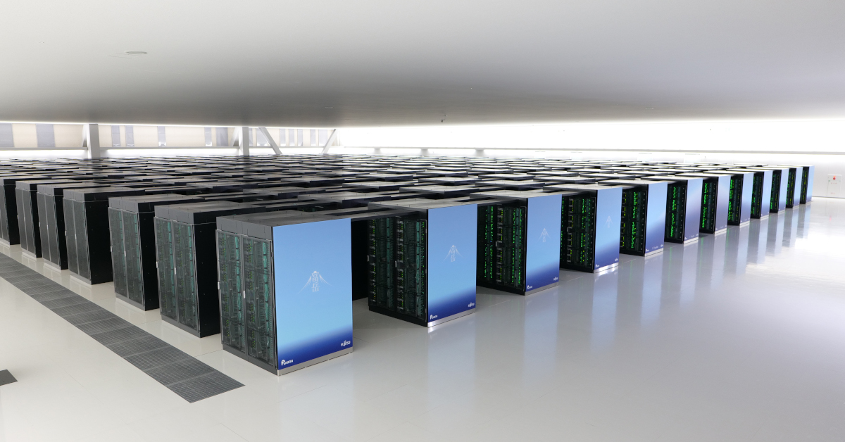
Had Intel's process been more in line, a similar Xeon line may have been possible. Fujitsu's A64FX gets its Flops with only 48 cores and 2.2GHz.
It's likely a better system than Summit but the perf/watt doesn't really improve and Summit is nearly 2 years old.
So yes, Apples 6xALU core family, SVE, AMX, Fujitsu A64FX and Zen3/Zen4, chiplet Alder Lake are all Jim Keller's babys maybe.
The problem with Phi was that it was too narrow, so it was bottlenecking it in real world HPC applications, and even in Linpack.
Yeah, I know, That was joke about K12 sold to FujitsuNo. A64FX is a very clear evolution of what Fujitsu was already building. It looks almost exactly like XIfx at a microarchitectural level, just enhanced. Fujitsu has a very clear uarch family starting from SPARC64 V, and they have iterated on it for specific products in the SPARC64, SPARC64fx (HPC chips prior to A64FX), GS, and now A64FX family.
A64FX also isn't particularly oriented toward general purpose loads. It is nothing like K12, lol.
View attachment 24046
View attachment 24047
")
I guess? Nearly every x86 design ever has been too narrow compared to GPGPU compute accelerators.

I just read the article, then read it again looking specifically for mention of power usage, and I saw nothing at all concerning power usage. Where did you see mention of power usage, in a separate article? If so, mind linking it for us?Very impressive, though I am a bit surprised at the power use.
I just read the article, then read it again looking specifically for mention of power usage, and I saw nothing at all concerning power usage. Where did you see mention of power usage, in a separate article? If so, mind linking it for us?
 www.top500.org
I assume you mean the 300A Celerons? Running at 450 Mhz, of course. Hmm, that means the in-order 1.6 Ghz Intel Atom CPU in an MSI Wind could complete the same task that the dual 450 Mhz 300A CPUs could, although it would take more like 10,000,000 years, instead of the speedy 1,000,000 years that the Celerons would take.My dual Celeron system can outperform that.
1,000,000 years Celeron vs. 1 second Fugaku
Heck no, nothing that blazing fast I'm taking Socket 370 Celeron.I assume you mean the 300A Celerons?
Thanks, I had clicked on that link, but only read the article. I had not noticed there was a list below the article, and wow, 28,300 KW is crazy, especially to not be running any GPUs, even moreso since they have not finished adding all of the nodes they're planning on having. They're going to be right at 30 MW, with all of the nodes. Still, once you realize it is up to 2.8X as fast as the 2nd-place system, the power numbers become much more in line with expectations.
Haha, those were reasonably fast (compared to their same-socket Pentiums), compared to the next generation Celerons, the Socket 478 Celerons. Those were absolutely hated, by more or less everyone.Heck no, nothing that blazing fast I'm taking Socket 370 Celeron.
I'd like to see how Fukagu efficiency stands against CPU only Xeon/Epyc systems:Thanks, I had clicked on that link, but only read the article. I had not noticed there was a list below the article, and wow, 28,300 KW is crazy, especially to not be running any GPUs, even moreso since they have not finished adding all of the nodes they're planning on having. They're going to be right at 30 MW, with all of the nodes. Still, once you realize it is up to 2.8X as fast as the 2nd-place system, the power numbers become much more in line with expectations.