For a good overview of gate-first versus gate-last HKMG implementation, here is a good thread to read:
http://forums.anandtech.com/showthread.php?t=2031334
Unfortunately a lot of the links in that thread have since gone dead as the publishers closed shop this spring.
If there were any questions left unanswered because of the dead links I would be happy to take a stab at answering them.
GloFo's 32nm HKMG on SOI implementation, the version tailored for AMD's products, does have two significant advantages over Intel's 32nm HKMG node...one obvious advantage is SOI. This "builds in" an intrinsic leakage reduction advantage which we all know and love since the day AMD started using it.
The second advantage, which doubles as a dubious honor, is that the engineering team will have had an extra year (plus a little more) to tweak and optimize the integration before it it was locked down and sent to Dresden for production ramp and qual.
The same sort of benefit that made the difference for AMD being able to use immersion-litho at 45nm versus Intel's situation where their production timeline was simply too aggressive to rely on immersion-litho so they had to opt for double-patterning.
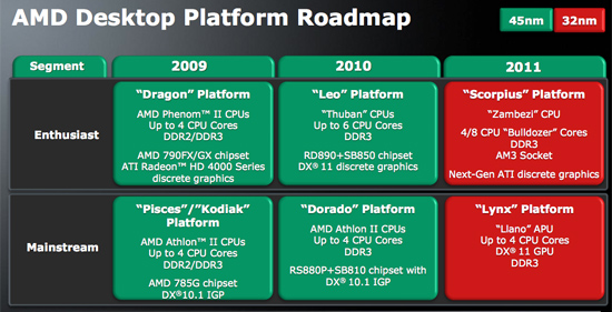
Right now, there is no Bulldozer model on the roadmap that will have a GPU on-die component. That doesn't mean that we won't see one circa 2012-2013, but right now it has not been announced.
This little factoid is rather interesting, isn't it? For all the "future is fusion" mantra AMD inundates their marketing slides with and yet all they talk about in enterprise/server (the big-margin product space) is bulldozer and an utter void of APU/Fusion SKU's. Is Fusion the future, or is bulldozer the future? And if fusion is the future then why bother buying today's products, or next year's bulldozer products? It is an odd marketing strategy imo.
Imagine if the ATI division had a marketing mantra "the future is holodock" but then went on to say "holodock products will not be available for the next 5-10yrs, in the meantime please purchase our already obsolete products that we are selling, they are obsolete because they can't create a holodock and we've already told you the future is holodock".
I just LOL everytime I see that "future is fusion" moniker on an AMD marketing slide where they are trying to tout the benefits of buying a non-fusion product. I may be the only one that sees the humor in this though.