
Info Forksheet (Post 3nm/Nanosheet) device info
- Thread starter soresu
- Start date
You are using an out of date browser. It may not display this or other websites correctly.
You should upgrade or use an alternative browser.
You should upgrade or use an alternative browser.

Further news on the possible Nanosheet device replacement called Forksheet.
Link here.
2nm is used as process name, but we all know that to be ambiguous at this point - I'd put it at Intel's 2nm rather than TSMC's.
Seems they could get 40% area improvement over Nanosheet, and 10% performance improvement.
It says 'performance', but does not specify if they mean 10% increased power consumption efficiency or 10% frequency increase for the same power.
I can only assume these percentages are at iso pitch.
Edit:
Found a quote "Compared to a nanosheet device, the researchers report a 10 percent speed gain (at constant power) and a 24 percent power reduction (at constant speed). "
Most white papers don't elucidate what is so special about either the mbcfet, or gaafet. While similar in most aspects to their finfet cousin, mbcfets use the quantum tunnelling property to drive electrons in its wake. Since the bottom source stacks are not conducting to the upper gate stacks - where most of the drive current travels - the static losses are at minimum, mbcfets are the last step until tfets which don't lose any in dynamic losses, too.
My father was formerly an electrical engineer until outsourcing nixed much of the British electronics industry, sadly whenever he talks like that it just goes way over my head.Most white papers don't elucidate what is so special about either the mbcfet, or gaafet. While similar in most aspects to their finfet cousin, mbcfets use the quantum tunnelling property to drive electrons in its wake. Since the bottom source stacks are not conducting to the upper gate stacks - where most of the drive current travels - the static losses are at minimum, mbcfets are the last step until tfets which don't lose any in dynamic losses, too.
I know just enough to find it interesting, and it certainly is - we probably won't see it (Forksheet device) in major production for at least another 5 years though.
The articles I have seen do not explicitly state that the Forksheet is in fact an MBCFET derivative - visually it looks more like they fused both MBCFET and a finFET structure into one.
What I consider most interesting about electron properties is, it has dual spin states whose axes are perpendicular and those are actually the only paths it takes at any time, so each time the electron jumps anywhere it is to either of these non-tracable(until perturbed) trajectories.
You could design a transistor where one electron jumps a quantum tunnel through spintronics. It is like planet orbitals in which you can specify the bands. Today, we mostly just pick the displacement of the projectile and hope for the best. In the future, the vector will be calculable, so it will tunnel the electron in 3D. So it will be a 3 bit device? I am no ee.
You could design a transistor where one electron jumps a quantum tunnel through spintronics. It is like planet orbitals in which you can specify the bands. Today, we mostly just pick the displacement of the projectile and hope for the best. In the future, the vector will be calculable, so it will tunnel the electron in 3D. So it will be a 3 bit device? I am no ee.
Most white papers don't elucidate what is so special about either the mbcfet, or gaafet. While similar in most aspects to their finfet cousin, mbcfets use the quantum tunnelling property to drive electrons in its wake. Since the bottom source stacks are not conducting to the upper gate stacks - where most of the drive current travels - the static losses are at minimum, mbcfets are the last step until tfets which don't lose any in dynamic losses, too.
While I haven't researched into the GAAFETs / MBCFETs yet, this explanation doesn't make sense to me or just isn't clear. Do you have a link or a paper reference that discusses this?
You need to know where the main body of current flows, it is at the top at the gate perimeter. Lack of physical contact between the drain and source make unexcited electrons unable to bridge the gap.
@~11:00, you can see the drive characteristics of a finfet. More voltage, more tunnelling there will be to the top fins.
@~11:00, you can see the drive characteristics of a finfet. More voltage, more tunnelling there will be to the top fins.
Last edited:
You need to know where the main body of current flows, it is at the top at the gate perimeter. Lack of physical contact between the drain and source make unexcited electrons unable to bridge the gap.
@~11:00, you can see the drive characteristics of a finfet. More voltage, more tunnelling there will be to the top fins.
I know how FINFETs work, I was asking about your comments on MBCFETs. Even this post it's unclear if you're talking about FINFETs or MBCFETs. You seem to be mixing the description of the two.
This IEEE entry describes it, but it's too recent to be free (Jan this year).I know how FINFETs work, I was asking about your comments on MBCFETs. Even this post it's unclear if you're talking about FINFETs or MBCFETs. You seem to be mixing the description of the two.
Edit: Found an abstract for it on another site.
"As the most feasible solution beyond FinFET technology, a gate-all-around Multi-Bridge-Channel MOSFET (MBCFET) technology is successfully demonstrated including a fully working high density SRAM.
MBCFETs are fabricated using 90% or more of FinFET processes with only a few revised masks, allowing easy migration from FinFET process. Not only on-target but also multiple Vt is achieved in challengingly limited vertical spacing between channels. Also, reliability of MBCFETs is shown to be comparable to that of FinFETs.
Three representative superior characteristics of MBCFET compared to FinFET have been demonstrated — better gate control with 65 mV/dec sub-threshold swing (SS) at short gate length, higher DC performance with a larger effective channel width (Weff) at reference footprint, and design flexibility with variable nanosheet (NS) widths.
The optimization of the standard cell design by using variable NS width is evaluated. The usefulness of MBCFET as a multi-purpose performance provider is proven by the modulation of effective capacitance (Ceff), effective resistance (Reff) and frequency by Weff control. Finally, mass production feasibility with MBCFET is proven through a fully working high density SRAM circuit."
Last edited:
@soresu Thank you, but I was specifically looking for links/papers based upon mtcn77's description about how they utilize quantum tunneling, there's no mention of this working principle in the linked paper. The description of source stacks and gate stacks also seems incorrect, or at least unclear to me in his description.
Definitely likely that I am clueless. Yes, I am mixing the two since there hasn't been any discrimination up until now.I know how FINFETs work, I was asking about your comments on MBCFETs. Even this post it's unclear if you're talking about FINFETs or MBCFETs. You seem to be mixing the description of the two.
Transistors don't follow Ohm's Law. Certain characteristics are transmuted at higher source-drain potentials. Normally, I would think the gate acts by blocking the flow, yet you see the opposite effect at high drive, current is moving against the resistance field. The current-resistance interface should have followed according to the fin diameter, again the opposite effect. The only possible interpretations are the gate's drive is making the resistance lower(not possible, resistance is a passive parameter of current flow), or it is causing breaks in the electromagnetic interface which causes electrons to skip across the tidebreaks at lower resistance. We already know when you give electron energy, it jumps. The only difference mbcfets will bring in my mind is, they will work at high drive current characteristically, not near the threshold voltage across the fin.
Normally, I would think the gate acts by blocking the flow, yet you see the opposite effect at high drive, current is moving against the resistance field.
No, the gate potential induces the current flow in the channel between source and drain. Not quite sure what you mean by resistance field.
The only possible interpretations are the gate's drive is making the resistance lower(not possible, resistance is a passive parameter of current flow), or it is causing breaks in the electromagnetic interface which causes electrons to skip across the tidebreaks at lower resistance.
You have to remember that these are semi-conducting materials and field effect transistors (FETs). Applying a potential on the gate creates an electric field which then allows for the formation of a conduction channel between source and drain. You seem to be under the assumption that current flows between the gate and channel? If so, this is not the case (ideally, realistically there will be a tiny amount of flow). There is an oxide layer between the gate and the substrate for this reason. This is also why silicon has been used so much despite other materials having higher mobility characteristics. It is easier to manufacture these devices with silicon and not have impurities or disruptions in the lattice that would allow for increased current flow to the gate. Quantum tunneling is a negative side effect of the FET structure that, in a very basic sense, causes electrons to move through barriers you've created to keep them out and this effect increases at smaller and smaller nodes given the same FET structure.
This is all a very basic overview of how it all works but this isn't the forum for a full discussion. This stuff is very complicated and involves a lot of physics both of Emag fields and quantum effects. I'm not a device physics expert by any means, but I took enough classes back in university and have to deal with it enough at the circuit design level that I can give basic explanations of how it works and the pros and cons of different types of transistors (bulk planar FETs, LDMOS, SOI, finFETs, etc.) and materials (SOI CMOS, GaAs, GaN, etc.). Nanowire FETs and nanosheet FETs (MBCFETs) I'm not as familiar with as they are still in the pipeline but from what I can gather, they still work very much the same as finFETs but basically going further into a 3D way of thinking/structure.
I totally get that the gate '"flow' induces it, but that is not how it happens. It still passes against the grain across where the resistance should be highest near the interface. That is not how V=IR explains it. It should have followed the near threshold conduction where resistance is lowest. I don't think transpositions are facultative in this case as R is passive to V and I, so it cannot have its own entity. If I were to describe V/R = I that would be why Ohm's Law does not work with transistors in the first place.No, the gate potential induces the current flow in the channel between source and drain. Not quite sure what you mean by resistance field.
Near the end, dear professor is going at length how that could be exploited for an on-state device. Consider for instance why have we had a wider gate interface at the invention of the finfet and why it has benefitted so much rather than not how planar transistors conduct electron flow? I'm under the assumption the minute etchings across the surface work towards your benefit to conduct through a band gap across the surface of the interface where - you guessed it - resistance is zero due to tunnelling effect rather than near threshold field conduction.You have to remember that these are semi-conducting materials and field effect transistors (FETs). Applying a potential on the gate creates an electric field which then allows for the formation of a conduction channel between source and drain. You seem to be under the assumption that current flows between the gate and channel? If so, this is not the case (ideally, realistically there will be a tiny amount of flow). There is an oxide layer between the gate and the substrate for this reason. This is also why silicon has been used so much despite other materials having higher mobility characteristics. It is easier to manufacture these devices with silicon and not have impurities or disruptions in the lattice that would allow for increased current flow to the gate. Quantum tunneling is a negative side effect of the FET structure that, in a very basic sense, causes electrons to move through barriers you've created to keep them out and this effect increases at smaller and smaller nodes given the same FET structure.
With all respect, I'm thinking maybe you are taking the electromagnetic field too literally. It's invisible spin state is totally against any solid interactions with physical matter and can jump across spaces.
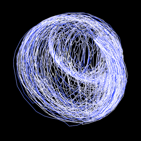
Suddenly I recalled why the electron image might interest you with incident information. You can read the original study at washington university. A discovery of this kind is not for the faint of heart. Given the right energy potential, you can gear electrons to their invisible gear forward. You just have to set the tunnel field trajectory straight where everything about quantum mechanics holds true. Otherwise, it won't act like a wavelength and would resist motion wasting your gate channel efforts with parasitic losses and etc. I'm not attune to that stuff.
[Washington state university]
I totally get that the gate '"flow' induces it, but that is not how it happens. It still passes against the grain across where the resistance should be highest near the interface. That is not how V=IR explains it. It should have followed the near threshold conduction where resistance is lowest. I don't think transpositions are facultative in this case as R is passive to V and I, so it cannot have its own entity. If I were to describe V/R = I that would be why Ohm's Law does not work with transistors in the first place.
There is no gate flow, that's the point, only gate potential. That potential creates an E-field which effects the electrons/holes in the material underneath by gathering the appropriate one towards the surface which then induces the conduction channel (or flow) between source and drain. BTW, ohms law is not just V=IR, that's the macroscopic version. It's been expanded more generally to have microscopic applications as well. This version has application in FETs.
Near the end, dear professor is going at length how that could be exploited for an on-state device. Consider for instance why have we had a wider gate interface at the invention of the finfet and why it has benefitted so much rather than not how planar transistors conduct electron flow? I'm under the assumption the minute etchings across the surface work towards your benefit to conduct through a band gap across the surface of the interface where - you guessed it - resistance is zero due to tunnelling effect rather than near threshold field conduction.
I can't watch the video right now to comment on it but will do so if I get time later.
With all respect, I'm thinking maybe you are taking the electromagnetic field too literally. It's invisible spin state is totally against any solid interactions with physical matter and can jump across spaces.
E-field and spin state are not the same thing. You're mixing your physics. Efields aren't "invisible" (obviously they are to the naked eye) but can be measured and mapped in space. Electron spin is something different. Also, when I talked about barriers, I was actually referring to energy barriers, not physical barriers (although the two aren't orthogonal to each other) but was trying to keep it simple as again, this isn't a physics forum and was just trying to get across the general idea.
Suddenly I recalled why the electron image might interest you with incident information. You can read the original study at washington university. A discovery of this kind is not for the faint of heart. Given the right energy potential, you can gear electrons to their invisible gear forward. You just have to set the tunnel field trajectory straight where everything about quantum mechanics holds true. Otherwise, it won't act like a wavelength and would resist motion wasting your gate channel efforts with parasitic losses and etc. I'm not attune to that stuff.
[Washington state university]
Show me any example of any practical application of this. It's great for research and to speculate about, but my point was that they are not controlling or guiding the quantum tunneling in MBCFETs as suggested. All of this stuff we have no practical application for yet that I am aware of.
Physical phenomena doesn't have to make even with our comprehension. That is what physics inquiry is for.There is no gate flow, that's the point, only gate potential. That potential creates an E-field which effects the electrons/holes in the material underneath by gathering the appropriate one towards the surface which then induces the conduction channel (or flow) between source and drain. BTW, ohms law is not just V=IR, that's the macroscopic version. It's been expanded more generally to have microscopic applications as well. This version has application in FETs.
I can't watch the video right now to comment on it but will do so if I get time later.
E-field and spin state are not the same thing. You're mixing your physics. Efields aren't "invisible" (obviously they are to the naked eye) but can be measured and mapped in space. Electron spin is something different. Also, when I talked about barriers, I was actually referring to energy barriers, not physical barriers (although the two aren't orthogonal to each other) but was trying to keep it simple as again, this isn't a physics forum and was just trying to get across the general idea.
Show me any example of any practical application of this. It's great for research and to speculate about, but my point was that they are not controlling or guiding the quantum tunneling in MBCFETs as suggested. All of this stuff we have no practical application for yet that I am aware of.
I don't think this is far off the shot with electron spintronics, but that is not the point of the debate. Spintronics aim subthreshold stochastic spiking of individual electron quantum states acting as the logic gate, however in this example every bit of the gate is part of the quantum device acting like a superconduction domain. The mere fact this has not been elaborated from normal conduction is the essence of the matter and I don't think it is the same as the rest of electromagnetic field. This goes mostly where conduction should not happen due to resistance, to my mind.
Physical phenomena doesn't have to make even with our comprehension. That is what physics inquiry is for.
I don't think this is far off the shot with electron spintronics, but that is not the point of the debate. Spintronics aim subthreshold stochastic spiking of individual electron quantum states acting as the logic gate, however in this example every bit of the gate is part of the quantum device acting like a superconduction domain. The mere fact this has not been elaborated from normal conduction is the essence of the matter and I don't think it is the same as the rest of electromagnetic field. This goes mostly where conduction should not happen due to resistance, to my mind.
Now we're getting off deep into the weeds. Using electron spin as bits (essentially) would be really cool but is also very off topic for this thread. I suggest we stick to the devices presented which we understand the physics of and know how to control in a practical way.
I understand you fully and suggest an alternative: compliance is unnecessary. The justification of the quantum electron field is here and now. Rather than debate and try imposing our will through rationalisations, we should let the elegant solution come about by its own expression in the outside world. Constant deduction by unit measure divided by unit value should give us the dimensionless magnitudinal expression we seek. Quantum phenomena are easier described than measured. It is too finite for any physical toolset.Now we're getting off deep into the weeds. Using electron spin as bits (essentially) would be really cool but is also very off topic for this thread. I suggest we stick to the devices presented which we understand the physics of and know how to control in a practical way.
Basically, we should let their practical applications demarcate what they are and eliminate what they are not. I say quantum tunnelling works in this context because we haven't bridged the gap between practical physics and quantum mechanics, albeit both features being unitary to the same physical 'electron' entity.
There are so many rules surrounding gate properties and channels not being too close yada yada yada. Well, duh, you need enough current to make some of the electromagnetic field fold unto itself, the crystal lattice etch gate interface form the elusive low impediment zone where electrons reach the upper orbitals making to the jump state. I cannot describe in any other way than saying it revolves around a certain ratio of gate length-width for this reason. There has to be a physical barrier to why electrons like square gates, but not triangulars.
Whatever your view on the topic, spintronic logic in mass production is at least 5-10 years away.I understand you fully and suggest an alternative: compliance is unnecessary. The justification of the quantum electron field is here and now. Rather than debate and try imposing our will through rationalisations, we should let the elegant solution come about by its own expression in the outside world. Constant deduction by unit measure divided by unit value should give us the dimensionless magnitudinal expression we seek. Quantum phenomena are easier described than measured. It is too finite for any physical toolset.
Basically, we should let their practical applications demarcate what they are and eliminate what they are not. I say quantum tunnelling works in this context because we haven't bridged the gap between practical physics and quantum mechanics, albeit both features being unitary to the same physical 'electron' entity.
There are so many rules surrounding gate properties and channels not being too close yada yada yada. Well, duh, you need enough current to make some of the electromagnetic field fold unto itself, the crystal lattice etch gate interface form the elusive low impediment zone where electrons reach the upper orbitals making to the jump state. I cannot describe in any other way than saying it revolves around a certain ratio of gate length-width for this reason. There has to be a physical barrier to why electrons like square gates, but not triangulars.
We will probably see it gain market share even as Forksheet increments and its vertical device successors are introduced, but it certainly won't just dominate overnight, it's just too different from the norm that processor architects are used to working on.
In all probability it will come hand in hand with a change from SRAM to some variant of MRAM for cache and persistent system memory.
In my last contribution, in this video doctor Aneesh goes on to differentiate between gate devices. If you scroll around 15:30, Finfet is the upside down perpendicular version of a double gated transistor and the gate at the end of the road is a gaafet.Whatever your view on the topic, spintronic logic in mass production is at least 5-10 years away.
We will probably see it gain market share even as Forksheet increments and its vertical device successors are introduced, but it certainly won't just dominate overnight, it's just too different from the norm that processor architects are used to working on.
In all probability it will come hand in hand with a change from SRAM to some variant of MRAM for cache and persistent system memory.
TRENDING THREADS
-
 Discussion Zen 5 Speculation (EPYC Turin and Strix Point/Granite Ridge - Ryzen 9000)
- Started by DisEnchantment
- Replies: 25K
-
Discussion Intel Meteor, Arrow, Lunar & Panther Lakes + WCL Discussion Threads
- Started by Tigerick
- Replies: 23K
-
 Discussion Intel current and future Lakes & Rapids thread
- Started by TheF34RChannel
- Replies: 23K
-

-

AnandTech is part of Future plc, an international media group and leading digital publisher. Visit our corporate site.
© Future Publishing Limited Quay House, The Ambury, Bath BA1 1UA. All rights reserved. England and Wales company registration number 2008885.