CPU Circuitry Layout Done By Hand/Computer

mike5757

Member
Apr 18, 2011
49
0
66
I was reading the Intel CPU Architect AMA over on Reddit (http://www.reddit.com/r/IAmA/comments/15iaet/iama_cpu_architect_and_designer_at_intel_ama/), and someone asked him if the CPU design is laid out by hand.

Here's his reply:
All of the analog circuitry, arrays, and performance-sensitive parts are definitely hand-drawn (schematics) and hand laid out. We're one of the few places that actually still do this (apparently Apple does too). You can tell which parts were laid out by hand if you look at die photos.

That begs for the question to be asked, how do you tell which parts were laid out by hand and which were done by computer?

EDIT: I've always thought of "begs the question" as being short for, "That previous statement begs for the following question to be asked."
 
Last edited:

Olikan

Platinum Member
Sep 23, 2011
2,023
275
126
thanks for the link, really cool read...

and...LOL, Intel architects reads semiaccurate :p
 

Tsavo

Platinum Member
Sep 29, 2009
2,645
37
91
Wonder what he means when he says, "once the fuses are blown, the change is not reversible."
 

Tsavo

Platinum Member
Sep 29, 2009
2,645
37
91
I wonder how they blow them.

Hand them to an intern that wears wool socks and shuffles feet when walking?
 

peonyu

Platinum Member
Mar 12, 2003
2,038
23
81
Wasn't one of the supposed problems with Bulldozer due to them not laying the design out by hand ?
 

dmens

Platinum Member
Mar 18, 2005
2,271
917
136
Synthesized layout looks random, hand-drawn layout looks structured.
 

Idontcare

Elite Member
Oct 10, 1999
21,118
58
91
The fuse is cut with a laser during packaging.

Intel still does laser-fuse? At TI we went away from laser-fusing and back to using electrical fuses exactly as their name implies - running a short-pulse of high voltage current through the fuse which truly "blows the fuse" same as one in the big-world sense, after which the circuit is permanently electrically open.

The benefit of electrical fusing over laser fusing is that the fuses don't have to be near the top of the stack, they can be buried and obscured by higher levels of metal.

The benefit of laser-fusing is that you rarely, if ever, get a failed fuse blow; whereas with electrical fusing you can get failed fuse blows (or only partial blows) in which case the supposedly disabled feature is still accessible.
 

dmens

Platinum Member
Mar 18, 2005
2,271
917
136
Intel still does laser-fuse? At TI we went away from laser-fusing and back to using electrical fuses exactly as their name implies - running a short-pulse of high voltage current through the fuse which truly "blows the fuse" same as one in the big-world sense, after which the circuit is permanently electrically open.

The benefit of electrical fusing over laser fusing is that the fuses don't have to be near the top of the stack, they can be buried and obscured by higher levels of metal.

The benefit of laser-fusing is that you rarely, if ever, get a failed fuse blow; whereas with electrical fusing you can get failed fuse blows (or only partial blows) in which case the supposedly disabled feature is still accessible.

I could be wrong, I'm a few years behind on that stuff. ;)
 
Last edited:

CTho9305

Elite Member
Jul 26, 2000
9,214
1
81
I was reading the Intel CPU Architect AMA over on Reddit (http://www.reddit.com/r/IAmA/comments/15iaet/iama_cpu_architect_and_designer_at_intel_ama/), and someone asked him if the CPU design is laid out by hand.

Here's his reply:

That begs for the question to be asked, how do you tell which parts were laid out by hand and which were done by computer?

EDIT: I've always thought of "begs the question" as being short for, "That previous statement begs for the following question to be asked."

It's really obvious once you know what you're looking for. Hand designs will generally have the design broken into many small pieces (because humans have to use a "divide and conquer" approach for large, complex things), and you'll see a lot of things neatly lined up. Auto-placed designs will either look almost entirely even, or will have blob-shaped patterns. Sometimes, designs are still broken into smaller pieces which get auto-placed, but that's less common (Intel seems to like that technique).

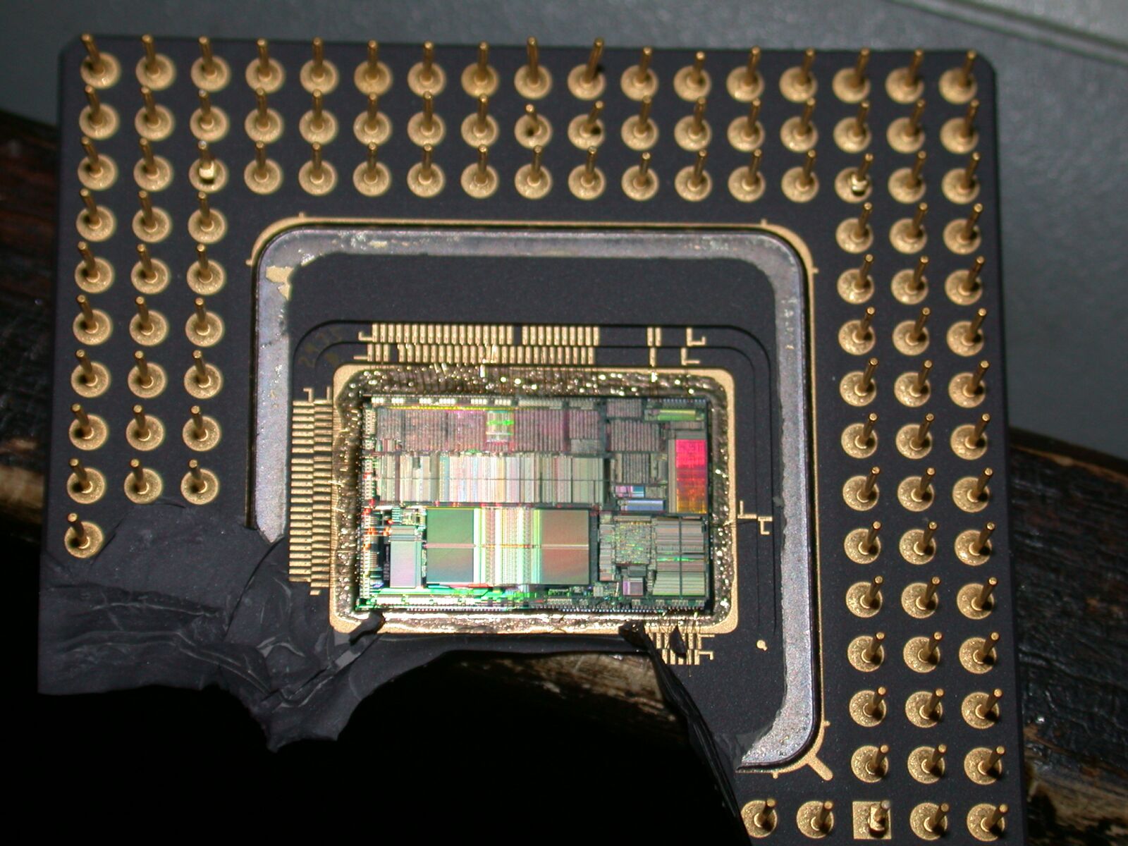
It's easiest to start with really old chips, so let's start with an Intel 486:
486-die2.JPG

See how things are lined up? The second row, and the stuff at the lower right are probably the best examples of what to look for in newer designs when you're trying to identify hand-designed modules

Jumping forward to Apple's A6:
74485_fig1.jpg

The blue part ("Dual ARM cores") is done by hand. Most of the rest is auto-placed (note the very even appearance).

Here's AMD's Llano; the GPU at the top is auto-placed, while the cores at the bottom are largely done by hand. Note the blobs in the GPU:
49142A_LlanoDie_StraightBlack.jpg


The little rectangular things scattered all over are memory arrays ("SRAMs"), and they'll always look like rectangles.

If you want to understand how the hand-placed designs end up looking the way they do, there are some examples showing how the engineers actually work in this PhD thesis. Page 137 (page 150 of the PDF) shows an excellent example (there's a color key on the next page). You can see how the design is "bit-sliced": each major chunk is made up of a one-bit slice that gets repeated left to right. Of course, the slices can't always be identical (most real logic functions aren't identical the whole way across the datapath), so it's not exactly the same in every slice, and sometimes the differences are significant (see the purple/pink stuff that's much narrower than the blue stuff? See the warts hanging off the right end?). You can tell that the designer picked pieces to do separately, and then assembled into the final result.

I wonder how they blow them.

Hand them to an intern that wears wool socks and shuffles feet when walking?

Just like a fuse in your car... you run a lot of current through the fuse, and it stops conducting (although the actual method of "failure" may be different - rather than just melting, it can be related to changes in crystal structure, or electromigration moving atoms around). You need a high voltage to blow fuses, so that usually comes from an external power supply connected to (possibly undocumented) pins in the socket, or gets generated on-die by a special circuit.
 

mike5757

Member
Apr 18, 2011
49
0
66
Wow. Thanks for the detailed reply, CTho9305. I usually notice the cache on processor dies (dice?) because of their huge and rectangular appearance, as you mentioned. That's about where my observations usually end, haha.

It looks like there's a lot of wasted space (the green areas) on the A6 die compared to most of the processors I've seen. Maybe because it's an SoC? Or maybe that green area actually serves a purpose.
 

Homeles

Platinum Member
Dec 9, 2011
2,580
0
0
I'd love to be able to point out where the ROPs are on a GPU. Pretty much every other structure I think I'm able to label correctly, but for ROPs, I have no idea.

And for CPUs, I wish I could figure out the front end.