Bigger Cores Instead of More Cores?

Wardrop

Member
Jul 30, 2011
38
0
66
Not being a micro-processor engineer, could someone possibly explain to me what's preventing manufacturers from making faster chips with less cores? Can you not just put more transistors in a single core, or is it a matter of diminishing return as the core gets bigger? Maybe something to do with yields?

With consumer 6-core and 8-core processors on the horizon, it does make you wonder why we're scaling out rather than up.
 

Arkadrel

Diamond Member
Oct 19, 2010
3,681
2
0
Like you said.... either scale up or out.

Why is everyone scaleing out instead of up (with 1 gigantic monolithic core?)? Good question... but I think the answear is one every chip maker knows the answear too and that is why your seeing chips that support more and more threads.

I suspect its simply more cost effective, to scale out... thus everyone is doing it.
Its a better way to make chips... coders just have to get used to designing software to run on more and more threads.

a eks. of this thats horrible, is starcraft 2..... its very cpu dependant and yet doesnt use more than 2 cores. I think blizzard had a brain fart when they did that one... atleast I hope so.
 
Last edited:

lol123

Member
May 18, 2011
162
0
0
Two things mostly:

1. Clock frequencies having reached a power wall at about 4 GHz, mostly due to increasing leakage power with smaller process nodes.
2. Diminishing returns when it comes to increasing IPC (instructions per clock). There have been large improvements to IPC in the last 5 years or so and with the release of Sandy Bridge it probably isn't possible to easily increase IPC at this time.

Arkadrel said:
I suspect its simply more cost effective, to scale out... thus everyone is doing it.
Its a better way to make chips... coders just have to get used to designing software to run on more and more threads.
It's a lot to ask from developers to transform problems that are inherently difficult to parallelize into ones that are not. The attitude, which I appreciate, from both Intel and IBM has been to engineer from the needs of developers rather than ask them to adapt to their idea of what computing should be like (which in my view Nvidia and lately also AMD are guilty of). Both Intel and IBM have responded to what large parts of the industry has demanded (fewer, fatter cores) and both are making truck loads of money at the expense of their competitors.

Going forward, I believe (though I might be mistaken) that Intel's tri-gate technology reduces leakage power and also operating voltage and the switching time of the transistors which should make it possible to have increases in clock frequency over 4 GHz.
 

Ken g6

Programming Moderator, Elite Member
Moderator
Dec 11, 1999
16,582
4,494
75
[thread=2174564]We discussed this kind of stuff before.[/thread]

Bulldozer is supposed to have every two cores share one FPU, which probably means that if both cores want to do AVX instructions they have to trade off between them. If the old disinformation about "reverse hyperthreading" were actually true, I imagine it would involve one core grabbing its neighbor's ALUs. If I were designing Intel's next Atom (which I'm not), I'd give each core a main pipeline and a simple-instruction pipeline like the original Pentium; then I'd let each core use the other's simple-instruction pipeline if the other core wasn't using it. It might get harder for more pipelines, though. Then again, there's this Intel Anaphase stuff that seems to involve software (static analysis?), at least partially.

I think the ultimate expression of this idea would be to have CPU "cores" as just instruction-reading-and-scheduling units. There could be a "pool" of ALUs that the cores use, and if only one core was running it could grab as many ALUs as the ILP of the code would allow. But because CPUs have to have at-least-64-wires-wide buses to transfer data, this is probably impractical.
 

BrightCandle

Diamond Member
Mar 15, 2007
4,762
0
76
Much of the original transistor budget went into making the CPUs faster. Partly it was on improving the algorithm so that it was quicker (but used more transistors) and a lot of it was about it running at increased clock speeds. Throwing more transistors at the problem only works if you have a better algorithm that you can move to, which they don't.

These days CPUs are actually cache memory with some processing logic attached, because cache is the most performant way to spend the transistor budget. But since the cores are relatively small things to add in comparison they throw them on there so that people can get more performance if they can use them. Intel could make a CPU on 40nm that had 12 cores on it (24 virtual threads) but it would have no cache and hence be much slower, especially in single threaded scenarios.

So actually I think today Intel and AMD are spending budget on the things they think improve single threaded performance the most and the other cores are freebies as there isn't much else to do with the transistors.
 

drizek

Golden Member
Jul 7, 2005
1,410
0
71
Going forward, I believe (though I might be mistaken) that Intel's tri-gate technology reduces leakage power and also operating voltage and the switching time of the transistors which should make it possible to have increases in clock frequency over 4 GHz.

No, the Tri-gate stuff is only marginally useful at high voltage. The main benefit is in reduced power consumption at low voltage/low frequency, which means Intel will probably be going the many-core way in the future.
 

greenhawk

Platinum Member
Feb 23, 2011
2,007
1
71
It is all tradeoffs with one feature being given preference over another.

As mentioned, the approach of going faster use to work well, but brings it's own issues (4Ghz?) as well as the situation that existed with the P4's (long pipelines).

While a easy thing to do (comparitivly), it has deminishing returns as 10% faster does not mean 10% better as the CPU spends longer waiting for information (cache offsets this, but you would need all your memory at cache speeds to eliminate it).

The next step is to be smart, but that means adding more transistors to implement new instructions (or better ways of doing the same task). Down side is that you are addressing features that most people might not use on a daily basis. This is where MMX/SSE came from, but you need the programers/complilers on your side as the new ways of doing something will not help overall performance at all if the code does not contains the new instructions.

The third option is the current one, and that is to add more cores. Only need the OS to reconize this as it moves the needed programs around and requires near no changes at the programming level compared to the program run on earlier hardware. Down side is that programming /compliers are needed to improve to make the most of the hardware (once again), but not as important as it was for new instructions.

The forth step that CPU manufactures will proberly want to address is one that will need a major change to the OS, so I am not expecting it very soon. That is to have OS support difference CPU cores. Currently the OS supports cores that are the same so task assignment does not matter but then you need to trade off large beefy cores (expencive) vs multiple small cores (cheap). Sort of like running a delivery company with either 1 large truck, or seveal small vans. Ideally for most, you want one of the large units and a few smaller ones for the normal daily grunt work.

AMD appear to have started a hybrid path in the direction of step 4 with the buldozer's FPU, but time will tell if tricking the OS into thinking their are more large FPUs present than their actually is vs the OS being aware of the truth (ie: like intel's hyperthreading). Of course, this is proberly going to be off loaded to the program and the OS will not care (selecting the correct pair will be interesting though).
 
Last edited:

Idontcare

Elite Member
Oct 10, 1999
21,110
59
91
...what's preventing manufacturers from making faster chips with less cores?

Nothing is preventing it. It is technically feasible and doable.

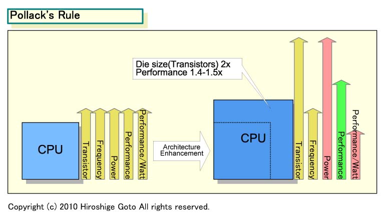
But it is more expensive to do in comparison to the current approach of "design one core, then copy-and-paste more cores as desired".

Take a quad-core chip, the core-logic design team spent four years making the core as functional as it is. How much longer would it have taken them if they had been asked to make just one core that was four times bigger and complex?

Read about Pollack's Rule, as exemplified by this chart by Goto-san:
05.jpg
 

wuliheron

Diamond Member
Feb 8, 2011
3,536
0
0
Nothing is preventing it. It is technically feasible and doable.

But it is more expensive to do in comparison to the current approach of "design one core, then copy-and-paste more cores as desired".

Take a quad-core chip, the core-logic design team spent four years making the core as functional as it is. How much longer would it have taken them if they had been asked to make just one core that was four times bigger and complex?


Its also more expensive simply because it is less flexible in almost every respect. If a quad core has a flaw in one core they can just sell it as a triple core. If they can't quite squeeze eight cores onto a die, they can reduce the number of cores. If adding a gpu or north bridge onto the chip provides more gains its easy enough to reduce the number of cores to make room.
 

ElFenix

Elite Member
Super Moderator
Mar 20, 2000
102,389
8,547
126
No, the Tri-gate stuff is only marginally useful at high voltage. The main benefit is in reduced power consumption at low voltage/low frequency, which means Intel will probably be going the many-core way in the future.

sounds like something intel will need to make their x86 offerings competitive with risc offerings in the mobile space.

could also make a larrabee type chip competitive in the HPC world.
 

Wardrop

Member
Jul 30, 2011
38
0
66
Interesting. I was under the impression that manufacturers would go for bigger cores, if they could, but it sounds as though they can, but they don't due to diminishing returns. It's not economical in other words.

The idea of having a large group of simple components is always attractive. It's desirable in pretty much all aspects of engineering, including programming, where breaking down your code into simple and specialized chunks makes the program easier to design, easier to maintain, and more flexible.

With that in mind, it's pretty clear that the future of computing will be many-core processors. In the distant future we have have many thousands of processing units per chip, similar I guess to GPU's.

This still doesn't solve the problem of calculations that require sequential processing, of course we'll naturally move away from such requirements by for example, redesigning our compression algorithms so small chunks can be decoded or encoded independently of everything else, unlike many of todays compression algorithms, but there will always be large operations that require sequential processing. Maybe 'in-order' is a better word than 'sequential'.
 

Idontcare

Elite Member
Oct 10, 1999
21,110
59
91
Interesting. I was under the impression that manufacturers would go for bigger cores, if they could, but it sounds as though they can, but they don't due to diminishing returns. It's not economical in other words.

The idea of having a large group of simple components is always attractive. It's desirable in pretty much all aspects of engineering, including programming, where breaking down your code into simple and specialized chunks makes the program easier to design, easier to maintain, and more flexible.

With that in mind, it's pretty clear that the future of computing will be many-core processors. In the distant future we have have many thousands of processing units per chip, similar I guess to GPU's.

This still doesn't solve the problem of calculations that require sequential processing, of course we'll naturally move away from such requirements by for example, redesigning our compression algorithms so small chunks can be decoded or encoded independently of everything else, unlike many of todays compression algorithms, but there will always be large operations that require sequential processing. Maybe 'in-order' is a better word than 'sequential'.

That's pretty much the nut of it. (and the word you are searching for is "serial")

Incremental clockspeed improvements, including the whole "turbo core" mania of late, are intended to improve the serial code performance.
 

lamedude

Golden Member
Jan 14, 2011
1,214
19
81
For Intel its probably the every feature made had to increase performance by 2% for every 1% increase in power consumption otherwise it wasn't allowed in the design rule (source).
 

Kristijonas

Senior member
Jun 11, 2011
859
4
76
I think the ultimate expression of this idea would be to have CPU "cores" as just instruction-reading-and-scheduling units. There could be a "pool" of ALUs that the cores use, and if only one core was running it could grab as many ALUs as the ILP of the code would allow. But because CPUs have to have at-least-64-wires-wide buses to transfer data, this is probably impractical.

That sounds perfect! There could be hundreds of cores this way and they could all work on only one "thread" (process) if needed. And at the same time they could work on thousand processes at the same time if it was more efficient that way.
 

DesiPower

Lifer
Nov 22, 2008
15,299
740
126
More heat/power wastage, efficiency issues. Think of why we have v6, v8 engines and not one huge cylinder.
 

sm625

Diamond Member
May 6, 2011
8,172
137
106
I dont see why they dont do reverse hyperthreading. The amount of transistors it would take to make it works seems like it would be less than a few million. All they need to do is link the schedulers so that one can see that the other is idle and in that case the branch predictor can use both cores' ALUs.
 

Idontcare

Elite Member
Oct 10, 1999
21,110
59
91
I dont see why they dont do reverse hyperthreading. The amount of transistors it would take to make it works seems like it would be less than a few million. All they need to do is link the schedulers so that one can see that the other is idle and in that case the branch predictor can use both cores' ALUs.

That sounds perfect! There could be hundreds of cores this way and they could all work on only one "thread" (process) if needed. And at the same time they could work on thousand processes at the same time if it was more efficient that way.

These are all feasible, nothing prevents them from being implemented now, but they are not power-efficient methods for extracting performance.

Keeping hundreds of ALU's powered up and accessible to the schedulers is going to consume power, requiring you to clock them all the lower. (see Nvidia Fermi GPU)

Same with reverse hyperthreading, its going to push up the power-consumption considerably, requiring you to clock the chip commensurately slower in order to fit it within a given TDP footprint.

This is why the efforts to implement turbo-core and power-gating were pursued.

TurboModeGraphic.png
 

JFAMD

Senior member
May 16, 2009
565
0
0
I dont see why they dont do reverse hyperthreading. The amount of transistors it would take to make it works seems like it would be less than a few million. All they need to do is link the schedulers so that one can see that the other is idle and in that case the branch predictor can use both cores' ALUs.

It comes down to the serial vs. parallel tasks.

Let's say you are making a salad. 2 chefs can split that task, one chops the lettuce, one cuts the carrots, etc.

Now, take that low level task like chopping a carrot. That is a singular serial task. You've seen the chef shows where the take a chef's knife and turn a carrot into tiny pieces in 4 seconds. Now, try to split that task between 2 chefs. Each one takes a chop and then hands the carrot back to the other guy for him to make his cut.

Imagine how long that will take.

The overhead of trying to synchronize a single task over multiple cores would take too long. The only way to really do that is to have a single scheduler over the two cores. But a shared scheduler creates a bottleneck.

Reverse hyperthreading is a pipe dream today because the task handling/communication overhead would make it unworkable.
 

GammaLaser

Member
May 31, 2011
173
0
0
One issue with making a monolithic die at such small nodes is the problem of interconnects. Assuming die size remains constant, you have smaller and smaller transistors being asked to drive signals across wires of shrinking widths, as a result delays goes up, creating speedpath issues. At some point wire delay overwhelms transistor delay and the node shrink advantages become negated. It would also affect the ability to apply power savings techniques to the clock trees and power domains when they span the entire die. In the first case the clock tree is tougher to manage so clock gating would be more difficult. In the second case its harder to power down parts of the chip without negatively impacting single-thread performance.
 
Last edited:

grkM3

Golden Member
Jul 29, 2011
1,407
0
0
intel has been increasing ipc with every shrink since the p4 days.sandy bridge is a monster and clocks like mad, I dont know what you mean but sandys are like 10-15% more powerfull than there older brothers and clock higher.

intel is giving us both,faster single core performance and with the etra space saved with smaller node they are giving us more faster cores in the same space.

Ivy is going to give us 50% less power draw as sandy at the same clocks so you can expect at least a 400mhz speed bump with ivy plus 2 more cores added on the ivy extreme 2011 platform.

haswell will offer another 10-20% increase of single core performance on top of Ivy

sandys memory system is unreal also for dual channel,Im getting 26000 mb/sec with 4 sticks installed on the board.once socket 2011 comes out that will double to 50gb/sec so when they put out the 10 core ivy we will have plenty of bandwidth to fill all those cores.

socket 2011 is by far the biggest upgrade.It took 50 years to hit 25-28gb memory bandwith and in one year intel is going to double it,add pcie 3.0 give us unlocked bckl along with quad channel 2133 support.

The platfrom will be able to run 6 of the fastest SSD drives in raid and it wont even push the system

Here is a thought to kinda get where we are heading,sandy bridge is a quad core like the old 65nm core 2s but has a 70% higher ipc in most benches at the same clocks and uses half the power.So at least intel is not just slamming more cores on a packege and going the more threads way like AMD is,they are actually raising single core performnce with every new Arch.
 
Last edited:

Idontcare

Elite Member
Oct 10, 1999
21,110
59
91
One issue with making a monolithic die at such small nodes is the problem of interconnects. Assuming die size remains constant, you have smaller and smaller transistors being asked to drive signals across wires of shrinking widths, as a result delays goes up, creating speedpath issues. At some point wire delay overwhelms transistor delay and the node shrink advantages become negated. It would also affect the ability to apply power savings techniques to the clock trees and power domains when they span the entire die. In the first case the clock tree is tougher to manage so clock gating would be more difficult. In the second case its harder to power down parts of the chip without negatively impacting single-thread performance.

Interconnect is essentially a cost issue.

There's a reason today's CPU's have 10-11 metal levels and not 3-4 and not 30-40.

The push for lower and lower k-value dielectrics is out of a desire to arrive at the lowest amount of delay while developing a node that has the least amount of metal levels as possible.

But don't kid yourself, when push comes to shove if the propagation delay becomes rate-limiting in the IC's performance they will, as they have time and again, simply add more metal levels (and commensurately more cost) to the design.

Don't you remember when they did this with the original 130nm thoroughbred (palomino) which had a version A and a version B where the version B added a metal layer to reduce heat and increase clockspeeds?

There are two versions of this core, commonly called A and B. The A version was introduced at 1800 MHz, and had some heat and design issues that held its clock scalability back. In fact, AMD wasn't able to increase its clock much above Palomino's top grades. Because of this, it was only sold in versions from 1333 MHz to 1800 MHz, replacing the larger Palomino core. The B version of Thoroughbred has an additional metal layer to improve its ability to reach higher clock speeds. It launched at higher clock speeds.
http://en.wikipedia.org/wiki/Athlon#Thoroughbred_.28T-Bred.29

That's not to say that everything in the BEOL can be solved by simply bolting on more metal levels, but the doomsday scenarios that are conjured up by projections of traditional scaling limitations are over rated IMO and IME.
 

pm

Elite Member Mobile Devices
Jan 25, 2000
7,419
22
81
One thing about large complex designs that I haven't seen mentioned is validation. IThe problem isn't just in the design of a large complex chip, but also functionally validating it. By "validation" I mean making sure that it's bug-free (or as close to bug-free as is feasible and cost-effective). The more complex a design, the harder it is to validate that all of the possible logic paths will actually work like they are supposed to. If you just rubber stamp out a couple of cores, you just need to check that one works and then check again that your fabric that connects them also works. A much easier task than a design that is 4-8x more complex because you widened the resources and then came up with a massive scheduler to feed it. I'm always amazed at the amount of time and engineering resources that go into functional validation. A bigger more complex core isn't really a circuit design problem - it's a functional design and validation problem

One issue with making a monolithic die at such small nodes is the problem of interconnects. Assuming die size remains constant, you have smaller and smaller transistors being asked to drive signals across wires of shrinking widths, as a result delays goes up, creating speedpath issues. At some point wire delay overwhelms transistor delay and the node shrink advantages become negated. It would also affect the ability to apply power savings techniques to the clock trees and power domains when they span the entire die. In the first case the clock tree is tougher to manage so clock gating would be more difficult. In the second case its harder to power down parts of the chip without negatively impacting single-thread performance.

In addition to the comments by IDC, as wire widths have shrunk, their height has gone up. Cross-sectionally, wires nowadays are much taller than they are wide (see http://www.realworldtech.com/includes/images/articles/iedm08-08.jpg). And most clock trees nowadays are clock grids. There are exceptions to this (I worked on one of those exceptions) but mostly nowadays, it's all gone to grids. Once you have a grid, you have resistances in parallel and life is easier. Then gating occurs at the block level or sometimes lower and you just tap off the grid and stick a fancy NAND gate on it to gate it.

As far as cross-block speedpaths, you can always increase the separation and width of the wires - they don't have to be minimum pitch. Just because you can make a wire super-thin doesn't mean you need to keep in minimum pitch to do a long route. Just widen the wires, or move to higher levels and you can solve the delay problem, then contact down in minimum pitch in M1 but then higher levels can be farther apart. You do what you need to to make noise and timing and widening wires is a good tool. The high level metals are beautiful from an electrical delay perspective... if your minimum pitch M1/M2 look lousy, just jump up a couple of levels... or, since custom design has disappeared like clock trees did, you can have your place and route tool solve the problem for you automagically.
 
Last edited:

GammaLaser

Member
May 31, 2011
173
0
0

I must be based off obsoleted/no longer true info, part of my original claims were based on data like these:

figure1.gif

http://www.copper.org/publications/newsletters/innovations/2006/01/copper_nanotechnology.html

Maybe this trend does not continue today because of more wire height/layers as you guys mentioned.

And also some interconnect delay-related research by Intel:

Intel has one chief goal for 3D integration: reducing the length of metal interconnects. Therefore face to face stacking was chosen by Intel, as it minimizes the inter die interconnect distance. It reduces the length and latency of the inter die vias – as well as their width – since they do not have to tunnel through the silicon substrate of each die, like in a face to back arrangement. This denser arrangement places more transistors within a clock cycle of each other, reducing global metal interconnect latency as a proportion of cycle time, as well as improving overall power consumption. Reducing the metal wiring between functional unit blocks results in a processor design that is limited more by transistor switching than interconnect delay. In this particular instance, Intel achieved both higher frequency operation as well as fewer pipeline stages [14].
http://realworldtech.com/page.cfm?ArticleID=RWT050207213241&p=7

Admittedly, that was based off the P4 so generalizations cannot always be made.

Anyway, not surprising that technology moves too fast for me yet again. :p

Although I wonder if the premise still remains: is it cheaper to add several more interconnect layers to fix delay problems on a big single-core or simply change the architecture to have multiple small cores, limiting the need to route between different parts of the die.
 
Last edited:

Idontcare

Elite Member
Oct 10, 1999
21,110
59
91
I must be based off obsoleted/no longer true info, part of my original claims were based on data like these:

figure1.gif

The thing to realize you have to account for with these types of "technology comparison" graphs is that they are created while normalizing a whole host of other IC parametrics constant in the background.

Reality is far more complex.

It is graphs like the one you referenced above which foretold the end of scaling 2 decades ago if we wanted to talk about going below 1um.

The graphs are legit, the data behind them are solid, but the problem is that they are prone to all manner of incorrect interpretation and projection.

I only know to recognize this because I've been on both sides of the fence, the outsider yearning to understand what all the engineers were yammering on about in terms of Moore's law really being about economics rather than technology and then on to becoming one of those engineers who was doing the yammering.

I've been involved with ITRS committees, led JDP's, heck I was even awarded a $2m grant to by the NSF to develop next-next-gen interconnect technologies...I wouldn't call "it" all a smokescreen, but to say that the future is either Plan A (insert doomsday scaling graph here) or nothing at all is a fairy tale that is certainly promulgated in the industry because sometimes it benefits you to forever play the part of the beggar. I definitely would not have had the opportunity to make my pitch to the NSF if I didn't have some doom and gloom scenarios about the future of CMOS technology to show.

Think of the space race, get a man on the moon first. In hindsight it was kind of a silly platform for why we "had" to do it, or else. But the ends justified the means, there was a lot of benefit to come from having done it.

Interconnect doom and gloom is kind of like that IMO. I've seen how the industry works, been part of the system. Been on the hamster wheel and climbed back off it. The challenges exist, make not doubt about it, but in the end the challenges are merely about generating options, alternative solutions, then the accountants come in to do their magic and decide for the engineers which of the solutions makes the most sense to the business that paid for the R&D to generate those options.

But fear is a good motivator. So we'll keep making those doom and gloom graphs to show academia, to show congress, to show our bosses, so we get the resources we feel we need to do the kinds of R&D we want to do. That's just business as usual.
 
Last edited:

Tuna-Fish

Golden Member
Mar 4, 2011
1,624
2,399
136
I dont see why they dont do reverse hyperthreading. The amount of transistors it would take to make it works seems like it would be less than a few million. All they need to do is link the schedulers so that one can see that the other is idle and in that case the branch predictor can use both cores' ALUs.

The register files that the two ALU clusters use are separate. Merging them wouldn't be something that costs just a few million transistors -- it might well be impossible to merge them without losing clockspeed, ports, or something else.