
[Ashraf] 10nm "Lakefield" SoC with Intel big + little cores
Page 2 - Seeking answers? Join the AnandTech community: where nearly half-a-million members share solutions and discuss the latest tech.
You are using an out of date browser. It may not display this or other websites correctly.
You should upgrade or use an alternative browser.
You should upgrade or use an alternative browser.
- Nov 14, 2011
- 10,513
- 5,994
- 136
If the Atom has a Sunny Cove CPU this means this Atom also has AVX-512?!
Unless this implementation of Sunny Cove has AVX disabled/removed. Intel make lots of Pentium chips with AVX disabled!
Unless this implementation of Sunny Cove has AVX disabled/removed. Intel make lots of Pentium chips with AVX disabled!
They did that for market segmentation, i dont think that would be the case here. But it may have it disabled or removed due to power concerns.
If the Atom has a Sunny Cove CPU this means this Atom also has AVX-512?!
Tremont only supports SSE actually. Intel did add a "Fast Read Processor ID" function to allow for the application to in theory switch between using AVX+ and SSE based upon what core it is running on.
darkswordsman17
Lifer
- Mar 11, 2004
- 23,444
- 5,852
- 146
BTW, I thought it a bit and thought that perhaps the customer is Microsoft for a Surface, but probally not. Maybe for an industrial use that would need the GPU for some reason and wants/needs very low idle. So lowish volume but something that would be doable with even super terrible yield.
They said OEM, so I wouldn't think this is industrial. I guess technically it'd be feasible still, but sounds like they think other companies might consider using this as well.
My guess: updated HoloLens, as it was already using an Atom based chip if I remember right. And other OEMs might consider putting it into standalone Mixed Reality headsets and leverage the HoloLens development (the bit about them offering it to other OEMs, I think they did the same thing with the chip they made for the original HoloLens but no one else was interested, probably because it wasn't a terribly interesting chip and so ARM designs were likely pretty appealing in comparison).
https://www.anandtech.com/show/11705/intel-eols-atom-chip-used-for-microsoft-hololens
Not sure what Google has for AR. I think Glass was using ARM, so I'd think they'd probably keep ARM, especially since they'd be looking to integrate their own stuff.
Andromeda?
Is that the product that's supposed to be based on the Courier design? That could be a possibility. I suppose maybe one of those tablets that use both a normal display and e-Ink, so that in book mode it'd use very little power too.
My thought as well. What customer would be big enough for intel to invest this much into desing such a SOC?
Best guess I can come up would be HoloLens. It would let them continue on from the initial HoloLens, and the design of the chip would fit that use very well.
Nice scoop Ashraf
EDIT: This definitely sounds like a nice product for a portable gaming device- especially with the 64EU GPU, and Adaptive Sync support to help deal with any framerate dips.
")
That could be a possibility, but since Sony has I believe outright said they won't be making a new portable to replace the Vita, and Nintendo is set with the Switch (they have a tendency of sticking with a platform when its selling, and going from Tegra to this would be quite a change, and doubt it'd be a home system with how tailored it is for mobile), not sure who else. Possibly an Xbox branded Surface? Like basically a Switch ripoff, but it'd be able to run a lot of games already made for Xbox/Windows. Kinda doubt it but it would be interesting. Apple would use their own chips if they were going to make a gaming device. And I feel like most other companies would opt for ARM for cost reasons. I don't know who else would try to make a mobile product like that, that could command a high enough price to make this chip worth it. Possible that the price isn't that high (or Intel gives them a discount with this serving as an R&D thing for them so getting it into actual product would help possibly make a market for it and would let other companies know that Intel is open and able to make chips like that).
Update: Techreport says 25% reduction is at the same process.
This depends on whether Intel wants to sacrifice L3 latency. Having it on another die will do this. If they want to keep it in a ring bus then it'll all be on the same die.
The Intel patent which was related to Forveros had the mesh+L3 on the bottom die, but the example given was more aimed at Granite Rapids I think.
At 40 mm2, you do still in theory get over 300 good dies per wafer even at 4 defects/sqcm (super terrible).
DrMrLordX
Lifer
- Apr 27, 2000
- 23,158
- 13,252
- 136
I'm more fascinated by the fact that Lakefield is 10nm than anything else. I mean, it is, isn't it?
Intel wasn't even willing to do the 8160 on their 10nm, but Lakefield? No problem. Not sure how they made that decision . . .
Anyway this is a chip to watch, at least to provide guidance of what it is Intel will be able to do between now and 2021 when 7nm hits the streets.
Intel wasn't even willing to do the 8160 on their 10nm, but Lakefield? No problem. Not sure how they made that decision . . .
Anyway this is a chip to watch, at least to provide guidance of what it is Intel will be able to do between now and 2021 when 7nm hits the streets.
Arachnotronic
Lifer
- Mar 10, 2006
- 11,715
- 2,012
- 126
I'm more fascinated by the fact that Lakefield is 10nm than anything else. I mean, it is, isn't it?
Intel wasn't even willing to do the 8160 on their 10nm, but Lakefield? No problem. Not sure how they made that decision . . .
Anyway this is a chip to watch, at least to provide guidance of what it is Intel will be able to do between now and 2021 when 7nm hits the streets.
What makes you think 8160 isn't 10nm?
What makes you think 8160 isn't 10nm?
The rumor is they ported it to TSMC, because of 10 nm's crappy yield.
DrMrLordX
Lifer
- Apr 27, 2000
- 23,158
- 13,252
- 136
What makes you think 8160 isn't 10nm?
Because . . .
The rumor is they ported it to TSMC, because of 10 nm's crappy yield.
Ding ding ding! Winnar. But we don't know if it has anything to do with yields. Tiny little modems? No. Lakefield? Yes. Wait, what? If anything the modem should have been easier to fab on 10nm than Lakefield if yields are still in question.
Arachnotronic
Lifer
- Mar 10, 2006
- 11,715
- 2,012
- 126
Because . . .
Ding ding ding! Winnar. But we don't know if it has anything to do with yields. Tiny little modems? No. Lakefield? Yes. Wait, what? If anything the modem should have been easier to fab on 10nm than Lakefield if yields are still in question.
Uhm.
Apple’s 5G iPhone will come to market in 2020, a source with knowledge of Apple’s plans says.
Apple plans to use Intel’s 8161 5G modem chip in its 2020 phones. Intel hopes to fabricate the 8161 using its 10-nanometer process, which increases transistor density for more speed and efficiency. If everything goes as planned, Intel will be the sole provider of iPhone modems.
Intel has been working on a precursor to the 8161 called the 8060, which will be used for prototyping and testing the 5G iPhone.
https://www.fastcompany.com/90261969/source-apples-first-5g-iphone-will-arrive-in-2020
DrMrLordX
Lifer
- Apr 27, 2000
- 23,158
- 13,252
- 136
I mean:
https://www.extremetech.com/computing/276690-report-intel-will-outsource-chipset-production-to-tsmc
Not sure if fastcompany has better info than that. Hell fastcompany isn't even mentioning this:
https://www.techradar.com/news/apple-iphone-modem-future
https://www.extremetech.com/computing/276690-report-intel-will-outsource-chipset-production-to-tsmc
Not sure if fastcompany has better info than that. Hell fastcompany isn't even mentioning this:
https://www.techradar.com/news/apple-iphone-modem-future
IntelUser2000
Elite Member
- Oct 14, 2003
- 8,686
- 3,787
- 136
I am puzzled by the fact you think Lakefield being on 10nm is strange, when they'll get regular Icelake chips on 10nm. Lakefield also sounds like a product coming later, so it'll have had longer time for the process to mature.
This is unlike shipping 100 million modems to Apple, because they need to guarantee that number has to work.
Also, Digitimes isn't always reliable.
Again, you are saying assumptions as they are facts.
HoloLens doesn't have enough of a market to make a custom chip for it. You are talking tens of thousands at best. If a company did ask, it makes much more sense its bigger ones like HP. They even made a custom package chip with on-package XMM 7560 WiFi to use it in the Spectre Folio.
Also it starts making sense to make such hybrid chips. If done well it can offer an optimal configuration between high single thread and multi-thread with low TDP.
This is unlike shipping 100 million modems to Apple, because they need to guarantee that number has to work.
Also, Digitimes isn't always reliable.
At 40 mm2, you do still in theory get over 300 good dies per wafer even at 4 defects/sqcm (super terrible).
Again, you are saying assumptions as they are facts.
HoloLens doesn't have enough of a market to make a custom chip for it. You are talking tens of thousands at best. If a company did ask, it makes much more sense its bigger ones like HP. They even made a custom package chip with on-package XMM 7560 WiFi to use it in the Spectre Folio.
Also it starts making sense to make such hybrid chips. If done well it can offer an optimal configuration between high single thread and multi-thread with low TDP.
Last edited:
Dayman1225
Golden Member
- Aug 14, 2017
- 1,160
- 996
- 146
HoloLens doesn't have enough of a market to make a custom chip for it. You are talking tens of thousands at best. If a company did ask, it makes much more sense its bigger ones like HP. They even made a custom package chip with on-package XMM 7560 WiFi to use it in the Spectre Folio.
It might work as a proof of concept of Foveros and their big.LITTLE type implementation.
- Nov 14, 2011
- 10,513
- 5,994
- 136
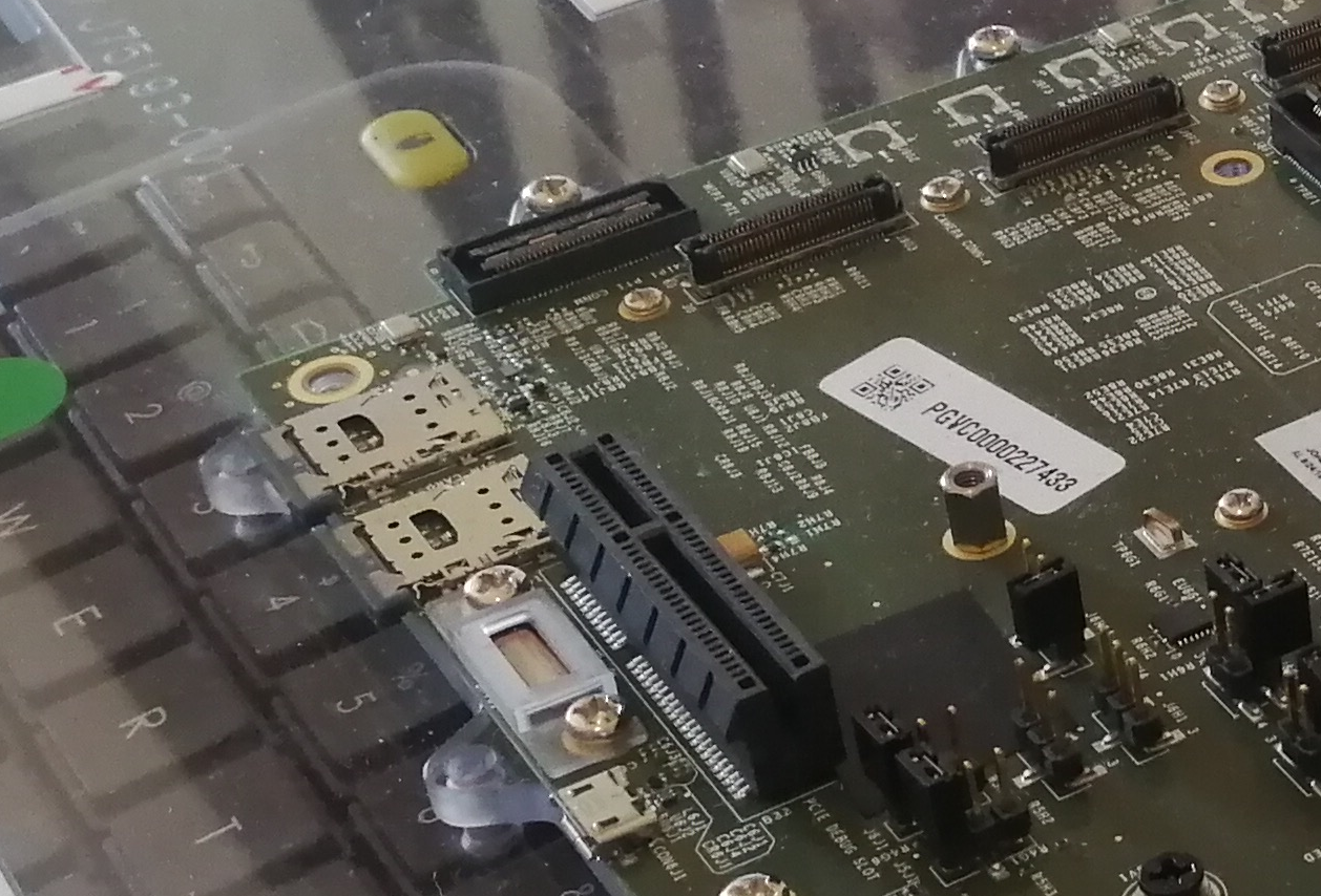
Looks like sim card slots on the Lakefield Dev/Validation board?
You can get LTE enabled versions of various Surface devices.
DrMrLordX
Lifer
- Apr 27, 2000
- 23,158
- 13,252
- 136
I am puzzled by the fact you think Lakefield being on 10nm is strange
Okay, I'll bite:
1). All of Intel's 10nm chips to date have had completely broken iGPUs. This product has a big one.
2). It seems like this product is moving along well in advance of IceLake-Y and IceLake-U, which are the next 10nm chips Intel will (probably) bring to market.
No idea on volume, but unless Intel feels like fabbing at a loss at low yields, I don't expect the volume to have any major impact on whether or not they'll be able to produce this product for profit. Seems like a pipecleaner for Intel's own version of DynamIQ.
IntelUser2000
Elite Member
- Oct 14, 2003
- 8,686
- 3,787
- 136
Okay, I'll bite:
1). All of Intel's 10nm chips to date have had completely broken iGPUs. This product has a big one.
Cannonlake is broken. Icelake is different. We do have leaks of Icelake-U parts with 64EUs already.
2). It seems like this product is moving along well in advance of IceLake-Y and IceLake-U, which are the next 10nm chips Intel will (probably) bring to market.
Let's look at few things we already know:
-Combination chips always take longer. Look at Kabylake-G, or AMD's Raven Ridge. Lakefield needs both Sunny Cove and Tremont to be ready.
-Ashraf has said Tigerlake achieves low idle power because it takes power management features from Lakefield. Tigerlake is a part coming after Icelake.
-Again, leaks. End of 2019, we'll see Icelake in some format. Whether its just -Y or -U and -Y we are not completely sure. We've seen Icelake and Gen 11 GPU in various formats from Geekbench and Sisoftware benchmarks.
The approximate timeframe of Lakefield hasn't even seen a leak, or even a rumor. You are possibly the first person that suggested that it'll arrive before standalone parts like Icelake.
- Nov 14, 2011
- 10,513
- 5,994
- 136
Okay, I'll bite:
1). All of Intel's 10nm chips to date have had completely broken iGPUs. This product has a big one.
Those were Gen10 GPUs; this is a Gen11. Maybe they tweaked the design to work around whatever problem they were having on 10nm? (Or maybe they finally fixed the process.)
Those were Gen10 GPUs; this is a Gen11. Maybe they tweaked the design to work around whatever problem they were having on 10nm? (Or maybe they finally fixed the process.)
IIRC In Gen11 Intel improved the flexibility in how many EUs can be disabled without disabling the whole thing. The Linux drivers for instance mention 48 and 32 EU versions of Icelake U and Y along with the 64. Intel to this point I think has only sold a rare couple of models with 1 EU disabled that isn't disabling the entire IGP.
DrMrLordX
Lifer
- Apr 27, 2000
- 23,158
- 13,252
- 136
Interesting point. But if Intel is pushing a 64 EU chip on 10nm with the option to disable EUs to account for poor yields, then how many total EUs do you think are baked in there to make sure that yields can remain high?
It almost seems like Lakemont would have to have more than 64 EUs per die to assure that every die could still have 64 working EUs. Or something like that.
We've had some leaked benches, but that's about it. Lakefield has been shown in greater detail that any potential IceLake-U or Y product. Also the leak goes back to what, April? With IceLake it's hard to nail down details outside of the scant information we've gotten from leaks. With Lakefield we're being told how many EUs it has, how many cores it has . . . this is stuff we've been wanting on IceLake for awhile (especially IceLake-S!) and instead we're getting it on Lakefield.
It almost seems like Lakemont would have to have more than 64 EUs per die to assure that every die could still have 64 working EUs. Or something like that.
The approximate timeframe of Lakefield hasn't even seen a leak, or even a rumor. You are possibly the first person that suggested that it'll arrive before standalone parts like Icelake.
We've had some leaked benches, but that's about it. Lakefield has been shown in greater detail that any potential IceLake-U or Y product. Also the leak goes back to what, April? With IceLake it's hard to nail down details outside of the scant information we've gotten from leaks. With Lakefield we're being told how many EUs it has, how many cores it has . . . this is stuff we've been wanting on IceLake for awhile (especially IceLake-S!) and instead we're getting it on Lakefield.
Last edited:
Interesting point. But if Intel is pushing a 64 EU chip on 10nm with the option to disable EUs to account for poor yields, then how many total EUs do you think are baked in there to make sure that yields can remain high?
64. The actual product could be partially disabled or they offer multiple options.
We've had some leaked benches, but that's about it.
Wrong. There is lots of activity for the Open Source and Linux support on pages such as freedesktop which is not the case for Lakefield.
Lakefield has been shown in greater detail that any potential IceLake-U or Y product.
I have to disagree, this is not the case. Intel didn't even confirm the architecture for Lakefield, they just confirmed 1 big core + 4 small cores. We know basically nothing about Tremont, assuming these are the smaller cores.
Also the leak goes back to what, April?
You clearly don't follow the page here, there are ICL-U ES entries on various pages like Furmark, 3dmark, Sisoft, Geekbench every few weeks. The last Geekbench entry from ICL-U was leaked in October. The first entries are very old, more than a year. Lakefield on the other side is dead at this point, we did get a broken screen from some twitter user but that's it. First driver entries as well, Lakefield has been added much later.
With Lakefield we're being told how many EUs it has, how many cores it has . . . this is stuff we've been wanting on IceLake for awhile (especially IceLake-S!) and instead we're getting it on Lakefield.
We know since ages that ICL GT2 features 64 EUs, the codename Lakefield wasn't even known at this point. Pretty sure ICL-U will be available before Lakefield.
TRENDING THREADS
-
 Discussion Zen 5 Speculation (EPYC Turin and Strix Point/Granite Ridge - Ryzen 9000)
- Started by DisEnchantment
- Replies: 25K
-
Discussion Intel Meteor, Arrow, Lunar & Panther Lakes + WCL Discussion Threads
- Started by Tigerick
- Replies: 23K
-
 Discussion Intel current and future Lakes & Rapids thread
- Started by TheF34RChannel
- Replies: 23K
-

-

AnandTech is part of Future plc, an international media group and leading digital publisher. Visit our corporate site.
© Future Publishing Limited Quay House, The Ambury, Bath BA1 1UA. All rights reserved. England and Wales company registration number 2008885.