Question 'Ampere'/Next-gen gaming uarch speculation thread

Page 100 - Seeking answers? Join the AnandTech community: where nearly half-a-million members share solutions and discuss the latest tech.

Ottonomous

Senior member
May 15, 2014
559
292
136
How much is the Samsung 7nm EUV process expected to provide in terms of gains?
How will the RTX components be scaled/developed?
Any major architectural enhancements expected?
Will VRAM be bumped to 16/12/12 for the top three?
Will there be further fragmentation in the lineup? (Keeping turing at cheaper prices, while offering 'beefed up RTX' options at the top?)
Will the top card be capable of >4K60, at least 90?
Would Nvidia ever consider an HBM implementation in the gaming lineup?
Will Nvidia introduce new proprietary technologies again?

Sorry if imprudent/uncalled for, just interested in the forum member's thoughts.
 

AtenRa

Lifer
Feb 2, 2009
14,001
3,357
136
But come on, a new node, a new architecture, and a new crazy high TDP - only for 3090 to be 50% faster than the 2080 TI? I don't buy that.

If the RTX 3090 Ampere is a conservative 30% more efficient than RTX 2080 TI Turing, that alone will translates into a 65% performance uplift over Turing based on the rumored TDP. So then 1.5 x 1.65 = 2.475, which is nearly 150% faster than the 5700 XT. But this is just at rasterization. Nvidia may (or may not) also hold a very commanding lead in RT capabilities.

I strongly believe Ampere architecture is more optimized for RT and ML than Raster performance,.
The new Tensor Cores on Ampere with native INT8/INT4, perhaps will need 2x the transistor count vs Turning Tensor Cores. So if they need 2x the transistor count plus they will increase the Tensor Core count vs Turning, then Tensor Cores will occupy a larger area percentage in Ampere vs Turing. Add extra RT cores, add extra bandwidth lanes for communication and a few other things and a lot of the die size goes to RT and ML performance increases and not for Raster.

For those reasons I believe that RTX3090 will need to increase clocks way above what they originally aiming for in order to reach the +60% over the RTX2080Ti. And that is why we have the TDP increase over Turning RTX2080Ti.
 
  • Like
Reactions: coercitiv

Ajay

Lifer
Jan 8, 2001
15,429
7,847
136
I strongly believe Ampere architecture is more optimized for RT and ML than Raster performance,.
The new Tensor Cores on Ampere with native INT8/INT4, perhaps will need 2x the transistor count vs Turning Tensor Cores. So if they need 2x the transistor count plus they will increase the Tensor Core count vs Turning, then Tensor Cores will occupy a larger area percentage in Ampere vs Turing. Add extra RT cores, add extra bandwidth lanes for communication and a few other things and a lot of the die size goes to RT and ML performance increases and not for Raster.

Are the registers in Turing's tensor cores 16b? Is Ampere going to 32b registers?
 

AtenRa

Lifer
Feb 2, 2009
14,001
3,357
136
Are the registers in Turing's tensor cores 16b? Is Ampere going to 32b registers?

I dont know about the registers but,

You need huge transistor allocation to have half the Tensor Cores per SM (4 Tensors per SM in Ampere vs 8 Tensors in Turing) and at the same time have 2x more FP16/FP32 throughput.
That means each Tensor core in Ampere has 4 times the performance of each Tensor Core in Turing.

From NVIDIA Ampere architecture

The A100 SM diagram is shown in Figure 7. Volta and Turing have eight Tensor Cores per SM, with each Tensor Core performing 64 FP16/FP32 mixed-precision fused multiply-add (FMA) operations per clock. The A100 SM includes new third-generation Tensor Cores that each perform 256 FP16/FP32 FMA operations per clock. A100 has four Tensor Cores per SM, which together deliver 1024 dense FP16/FP32 FMA operations per clock, a 2x increase in computation horsepower per SM compared to Volta and Turing.
 

Konan

Senior member
Jul 28, 2017
360
291
106
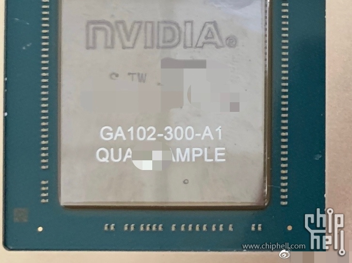
This one is huuuge

nvidia-geforce-rtx-30jwk0d.jpg


WCCFTech - NVIDIA GeForce RTX 3090 & RTX 3080 Ampere GA102 GPU Allegedly Pictured – Massive Die For Enthusiast Gaming Graphics Cards
The TW on the chip indicates Taiwan so TSMC? or maybe diffused in Korea and made in Taiwan ??
 
  • Like
Reactions: Krteq

Krynj

Platinum Member
Jun 21, 2006
2,816
8
81
As somebody that is currently waiting to pull the trigger on something in the $400/$500 range for my next build, should I expect any product announcement in that price range? Or will we just see price cuts to the current 20xx cards? The GPU is basically the last component I need before I pull the trigger on my new parts, so I was just looking for a bit of insight on what to expect. I haven't bought an Nvidia card in about 17 years, or built a system in about 8, so I'm a bit out of the loop to say the least.
 

Konan

Senior member
Jul 28, 2017
360
291
106
As somebody that is currently waiting to pull the trigger on something in the $400/$500 range for my next build, should I expect any product announcement in that price range? Or will we just see price cuts to the current 20xx cards? The GPU is basically the last component I need before I pull the trigger on my new parts, so I was just looking for a bit of insight on what to expect. I haven't bought an Nvidia card in about 17 years, so I'm not too familiar with their product launches.

This time next week we have a strong chance of learning official pricing and some product info from Nvidia in their event on Sept. 1.
Could be a RTX 3070/3060 in that price range
 
  • Like
Reactions: Krynj

Stuka87

Diamond Member
Dec 10, 2010
6,240
2,559
136
The TW on the chip indicates Taiwan so TSMC? or maybe diffused in Korea and made in Taiwan ??

'S TW' is for Samsung. Not TSMC.

EDIT: Correction, that's just where the final assembly took place. Its in no relation to where the chip was diffused. nVidia often has that on chips, but also sometimes has 'B KOREA' on the chip.
 
Last edited:
  • Like
Reactions: Konan

CakeMonster

Golden Member
Nov 22, 2012
1,389
496
136
35% for the steps listed there is very disappointing for a 2 year wait. Especially considering the price speculations.

I don't really believe it, but my qualifications are close to zero.
 

Glo.

Diamond Member
Apr 25, 2015
5,705
4,548
136
The thing that baffles me is...

No way Jenhsen will let it be this slow. Not compared to Navi 2. Nvidia Engineers know, (well they know 90-95% at this point...) how Navi 2 will behave. They can clock it to hell.

Why only 35%?

I don't buy it. It will be faster. Around 40-45% in 1080p, and faster in 4K.
 

Ajay

Lifer
Jan 8, 2001
15,429
7,847
136
I dont know about the registers but,

You need huge transistor allocation to have half the Tensor Cores per SM (4 Tensors per SM in Ampere vs 8 Tensors in Turing) and at the same time have 2x more FP16/FP32 throughput.
That means each Tensor core in Ampere has 4 times the performance of each Tensor Core in Turing.

From NVIDIA Ampere architecture
Thanks! Looking over that documentation; I think it’s pretty clear that for GA102, the total cuda core count will go down as will FP64 FMAs and number of tensor cores. I don’t think consumer TPUs will need fp64 either (unless A102 is also for engineering workstations as well). So I think some reasonable cuts can be made, especially if NV is aiming for higher clocks. Hopefully we’ll see actual products soon and know for sure.