AMD's efforts involved in moving to TSMC's N7, advantages for going with chiplets (warning: many images)

moinmoin

Diamond Member
Jun 1, 2017
4,950
7,659
136
I think this has been posted in four threads so far or something like that. Let's talk about these interesting slides in this dedicated thread instead.

@rickxross mentioned this Japanese article with plenty English slides about AMD's efforts involved in moving to TSMC's N7 7nm node.

@uzzi38 mentioned an article at WikiChip discussing the capabilities and challenges with going with 7nm.

The slides are from a talk by AMD's Teja Singh at the ISSCC 2020 (International Solid-State Circuits Conference, ended two days ago).

AMD improved switching capacitance by ~9% beyond the node change.
photo002_oeqkv6.jpg


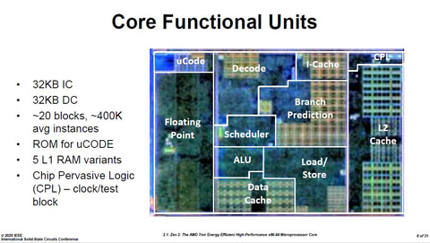
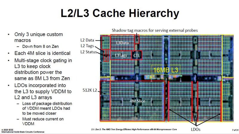
Slides include some annotated dies!
photo003_optkvl.jpg

photo004_obak19.jpg


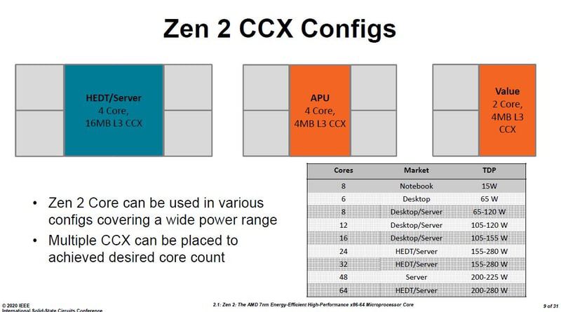
AMD doesn't mention desktop, instead it's HEDT/server.
photo006_o4fk74.jpg


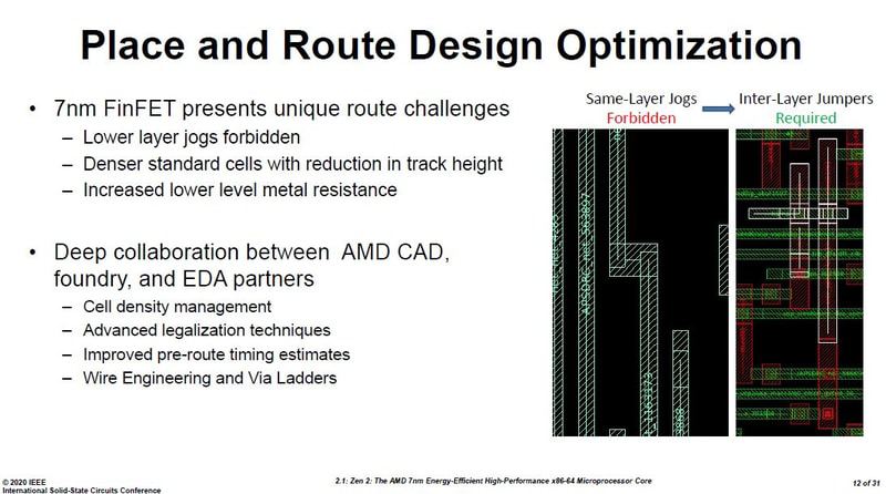
Layouting the placement of the differently sized cells is tricky, leaving many gaps.
photo009_olaj5t.jpg


Routing no longer can have corners at the same layer, instead requires 3D inter-layer jumpers.
photo010_oinkxa.jpg


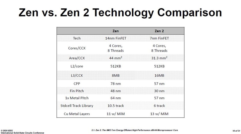
Switching capacitance improved a lot further from going from 14nm to 7nm node.
photo012_olckwy.jpg


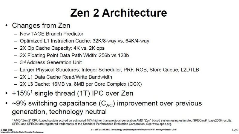
Summary of the perf/watt improvements.
photo013_o7mjm8.jpg


The resulting frequency/power curve.
photo014_ocxjlp.jpg


As well as the frequency voltage curve.
photo015_osqkhn.jpg


CCD = 3.8 bil FETs @ 74mm², Server IOD = 8.34 bil FETs @ 416mm², Client IOD = 2.09 bil FETs @ 125mm²
photo017_oozjay.jpg


Cost per yielded mm² for a 250mm² die doubled going from 14/16nm to 7nm.
photo018_onlj92.jpg


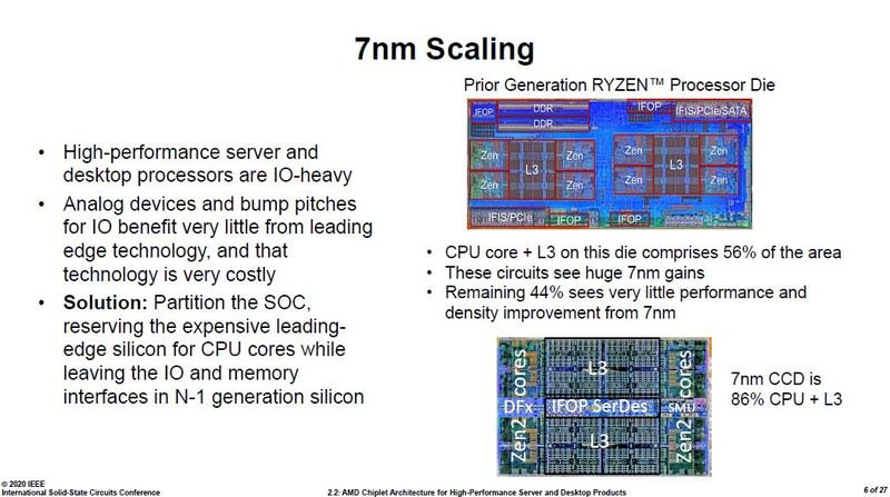
Zeppelin comprised of 56% core + L3$ area. CCD increased that to 86%.
photo019_ou3jf2.jpg


One more annotated die! Wonder what the SMU comprises of, is it ARM based?
photo020_or6jzs.jpg


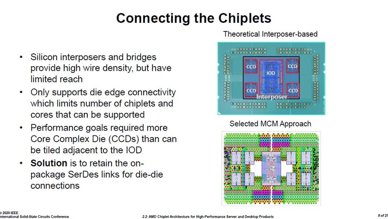
Interposer was under consideration, but dies would have to be much closer and only 4 chiplets would have combined then, limiting max core count to 32 compared to the 8 chiplets and 64 cores possible with the chosen MCM approach.
photo021_ocskvy.jpg


Improvements in the IFOP SerDes architecture.
photo022_oxuknk.jpg


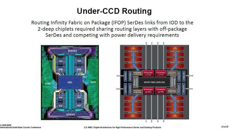
Annotated routing map, that looks cramped!
photo023_o4cjyc.jpg


And since CCD is 7nm and IOD is 14/12nm the bump pitch differ as well. Change to an interface that's compatible with both.
photo024_ojlkel.jpg


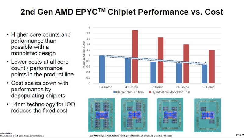
The resulting margin is bigger the more cores it is used for, pretty much the opposite than with monolith dies.
photo025_o08jyd.jpg


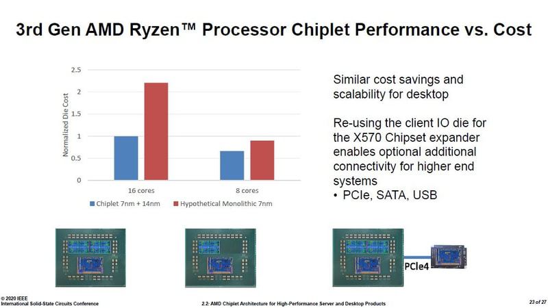
On desktop the difference is even more stark. These show AMD doesn't need to hold back with many cores, instead it would profit even more if people where to buy more of the most cores chips as those have way higher margins while the cost for the dies barely increases.
photo026_orpjif.jpg
 
Last edited:

cellarnoise

Senior member
Mar 22, 2017
712
396
136
AMD did the math and has good interconnect tech. Hope they continue to make bank.

Also hope Intel can get back in the game. Would be nice to see another 5 years of CPU advances before the manufacturing tech slows down further.
 

Vattila

Senior member
Oct 22, 2004
799
1,351
136
Interesting! The slides state that Zen 2 uses the N7 HD (6T) process variant (high density). It has been widely presumed it would use N7 HP (7.5T) for high performance.

Perhaps Zen 2 could have hit that 5 Ghz mark, if that was the priority. Now it seems power and area were more important.

photo007_o.jpg


Edit: 6T is also in this slide, so it is very unlikely to be a mistake.

photo013_o7mjm8.jpg
 
Last edited:

coercitiv

Diamond Member
Jan 24, 2014
6,199
11,895
136
Now it seems power and area were more important.
In hindsight it makes sense: Rome came with a big jump in core count, hence power and area were definitely the priority given the rather low clocks they needed to saturate TDP. Renoir is also about power & density. That leaves desktop in an awkward place, but no more than it's been in years.
 

NTMBK

Lifer
Nov 14, 2011
10,237
5,019
136
Some very interesting slides- thanks for making this thread! I wouldn't have seen them otherwise.

Interesting point about interposers limiting them to 4 dies. If Zen3 still has 8 core compute chips, I guess that will make the same design choice.
 
  • Like
Reactions: Tlh97 and lobz

moinmoin

Diamond Member
Jun 1, 2017
4,950
7,659
136
Some discussion about the slides from other threads:

Re: chiplets
Very interesting slides, thanks! It looks like AMD also considered interposer, but that would have limited CCD chiplet count to 4:
photo021_o.jpg


And where was that guy, claiming that chiplets will be replaced by monolithic design, as packaging is so expensive (but extra mask costs in million per each 7nm die are a sneeze):
photo026_o.jpg


photo025_o.jpg


Overall I really suggest checking these slides out, very informative.
What struck me when I first saw the slides was the increase in cost of higher die count CPUs. It's not just that it is cheaper to use chiplets, but that it becomes cheaper to a greater extent as the core count increases.

Meaning that until Intel goes to chiplets, AMD can squeeze them at will in higher core count CPUs.
Indeed, margin increases tremendously with the higher core counts. So for AMD (even ignoring the competition) it actually makes sense to push "ridiculous" amount of cores: 1) it increases their profit, 2) it increases their competitive edge, and 3) it makes software optimizations for more cores more likely to happen soon which again feed back into their competitive edge. The only limit it scalability of the hardware.

----

Re: switching capacitance
Thanks for the link, so far we know that Zen had 15% improvement over excavator in switching capacitance and Zen 2 added an additional 9%, that is very impressive indeed.
Good call. Wanted to ask for sources, but google already gave me an IEEE document abstract stating such as well. Looks like this is a steady focus by AMD which may well continue with Zen 3 and onward.

----

Re: core layout
photo003_l.jpg


Nice find from Panino

It surprises me how large the branch prediction unit is (as well as the decode) and how tiny the area for ALU.

Doesn't surprise me how huge the doubled up FPU is though.

Sadly, my guess for the functional units is way off.

I wonder if the layout for Zen3 will be radically different.
The Zen 2 core/uncore is commonly considered a direct evolution of Zen, with the packaging architecture and node switch being the big changes. Zen 3 should see bigger changes in the core layout, before Zen 4 with a new platform introducing PCIe 5 and DDR5 changes the surrounding architecture again. That's how I see it so far anyway.

----

Don't mock the amount of work that goes into getting a uArch into one of the smaller nodes.
Indeed. I really liked the slides on cell placement and route optimization since those are things often taken for granted unless they are spelled out like they are here. They also explain why Intel currently is incapable of using its design on multiple nodes, they don't have any standardization so reworking designs for different nodes equals to adapting much of the design itself. AMD needed to make such decisions as well, but they have plenty experience with that process already thanks to the steady semi custom work across multiple nodes in the last decade.
 

lobz

Platinum Member
Feb 10, 2017
2,057
2,856
136
Interesting! The slides state that Zen 2 uses the N7 HD (6T) process variant (high density). It has been widely presumed it would use N7 HP (7.5T) for high performance.

Perhaps Zen 2 could have hit that 5 Ghz mark, if that was the priority. Now it seems power and area were more important.

photo007_o.jpg


Edit: 6T is also in this slide, so it is very unlikely to be a mistake.

photo013_o7mjm8.jpg
I always thought it was HD and only Navi is HP.
 
  • Like
Reactions: Vattila

Vattila

Senior member
Oct 22, 2004
799
1,351
136
Interesting point about interposers limiting them to 4 dies. If Zen3 still has 8 core compute chips, I guess that will make the same design choice.

Perhaps this limitation has been overcome with TSMC's advances in packaging technology? Curiously, the test chip in the following article published last August consists of eight 75 mm² + two 600 mm² chiplets.


Boxer_1565180527.215269_asset.jpg
 
Last edited:

lobz

Platinum Member
Feb 10, 2017
2,057
2,856
136
Re: switching capacitance

Good call. Wanted to ask for sources, but google already gave me an IEEE document abstract stating such as well. Looks like this is a steady focus by AMD which may well continue with Zen 3 and onward.
This is a much bigger deal than anyone would think at first glance. Zen 1 already had an exceptionally high power efficiency, especially considering it was made on a technically inferior node compared to Skylake, and I bet the improved switching capacitance played a major role. Improving another 9% on top of that just architecturally is no small feat. This is not a low-hanging fruit that's easy to naturally and evolutionally find.
 

lobz

Platinum Member
Feb 10, 2017
2,057
2,856
136
Perhaps this limitation has been overcome with TSMC's advances in packaging technology? Curiously, the test chip in the following article published last August consists of eight 75 mm^2 + two 600 mm^2 chiplets.


Boxer_1565180527.215269_asset.jpg
That's incredible and I'm sure it will end up being used some time soon! However, even with the current Epyc's size, I think it would have had a cost of at least 2-3x at the time the design was finalized. The best thing is, as it turned out, the actual impact of the latency tradeoffs were nowhere near as severe as they were supposed to be on paper, not in the majority of real world workloads at least.
 
  • Like
Reactions: Vattila

lobz

Platinum Member
Feb 10, 2017
2,057
2,856
136
Effectively, regarding the Libraries, AMD got High Performance CPU on a Low-Power node.

Which in itself is quite the achievement. One of the best physical designs of past years.
Imagine them going less dense and overall much less power efficient for having another 200 MHz at low threaded boost frequencies.
It turned out great and I'm perfectly content with haters citing single digit % average fps advantage on the overpriced 9900K/KS in retaliation.
 
  • Like
Reactions: lightmanek

Glo.

Diamond Member
Apr 25, 2015
5,707
4,552
136
Imagine them going less dense and overall much less power efficient for having another 200 MHz at low threaded boost frequencies.
It turned out great and I'm perfectly content with haters citing single digit % average fps advantage on the overpriced 9900K/KS in retaliation.
Another 200 MHz would not do much for gaming :). Zen2's Gaming bottleneck comes from relatively slow Cache bandwidth.
 
  • Like
Reactions: uzzi38 and lobz

lobz

Platinum Member
Feb 10, 2017
2,057
2,856
136
Great OP and posts.

Looking at the ucode and decode areas [2nd slide here], that patent concerning pushing least used ucode to the L1 and L2 in order shut down the decode circuitry more often seems like a way of significantly reducing total core power.
Also a very good catch. While it doesn't always work that way, statistically it reduces the power actually used by a lot. All these things work together for Zen 2 to be a massively more efficient architecture than the latest Core irregardless of the process node.