AMD summit today; Kaveri cuts out the middle man in Trinity.

Page 3 - Seeking answers? Join the AnandTech community: where nearly half-a-million members share solutions and discuss the latest tech.
Status
Not open for further replies.

AtenRa

Lifer
Feb 2, 2009
14,003
3,362
136
I didn't say flagship Kepler chip, I said flagship consumer product. The point is that it makes no sense whatsoever to say that NVIDIA pursues "more GPGPU oriented devices" when leaving out the GTX 680 and GTX 690. And there is no indication that the lower models will have any better GPGPU efficiency.

The problem is that you compare the GTX580(GF110) against the GTX680(GK104). GF110 was the Flagship Fermi chip when GK104 is not the Flagship Kepler chip.

GK104 (GTX680) is faster than GF114 (GTX560Ti) in every GPGPU application. GK104 is even faster than GF110(GTX580) in certain computational tasks like DX-11 compute shader. GK110 will be the next consumer flagship from NVIDIA.

You have to realize that even GTX560Ti was not that much oriented for GPGPU like its big sister GF100/110 Fermi. But GF104/114 was not the flagship consumer Fermi chip, it was the GF100/110.

It was the turn AMD took with Tahiti in GPGPU that made possible for NVIDIA to put the middle chip GK104 as the high end consumer chip. Combined with the new 28nm TSMC low yields low capacity they took the opportunity and it paid them well.

Now we pay more for middle end GPUs but that is another story ;)
 

Abwx

Lifer
Apr 2, 2011
11,885
4,873
136
ROTFL, like being only 64-bit (2 packed floats) vs 128-bit (4 packed floats) with SSE

Surely of great use since the Cpus of the time couldnt
execute four floating point instruction per cycle...

Indeed , Athlon CPUs were superior to Pentium3 for
floating point.
 

bronxzv

Senior member
Jun 13, 2011
460
0
71
Surely of great use since the Cpus of the time couldnt
execute four floating point instruction per cycle...

in other words your consider the SSE *ISA* as technically inferior because it was forward thinking

next time you'll tell me that you miss the infamous x87 stack aliasing and the EMMS instruction ?
 

Abwx

Lifer
Apr 2, 2011
11,885
4,873
136
in other words your consider the SSE *ISA* as technically inferior because it was forward thinking

next time you'll tell me that you miss the infamous x87 stack aliasing and the EMMS instruction ?

At least ,before rounding , X87 was 80bit precision when SSE2
was 64bit precision.....;)

As for who had superior SIMD set , well , 3Dnow did predate
SSE , so surely that being more recent the latter was more complete.
 
Last edited:

piesquared

Golden Member
Oct 16, 2006
1,651
473
136
Saw this in Phoronix forums:

Existing APIs for GPGPU are not the easiest to use and have not had widespread adoption by mainstream programmers. In HSA we have taken a look at all the issues in programming GPUs that have hindered mainstream adoption of heterogeneous compute and changed the hardware architecture to address those. In fact the goal of HSA is to make the GPU in the APU a first class programmable processor as easy to program as today's CPUs. In particular, HSA incorporates critical hardware features which accomplish the following:

1. GPU Compute C++ support: This makes heterogeneous compute access a lot of the programming constructs that only CPU programmers can access today

2. HSA Memory Management Unit: This allows all system memory is accessible by both CPU or GPU, depending on need. In today's world, only a subset of system memory can be used by the GPU.

3. Unified Address Space for CPU and GPU: The unified address space provides ease of programming for developers to create applications. By not requiring separate memory pointers for CPU and GPU, libraries can simplify their interfaces

4. GPU uses pageable system memory via CPU pointers: This is the first time the GPU can take advantage of the CPU virtual address space. With pageable system memory, the GPU can reference the data directly in the CPU domain. In all prior generations, data had to be copied between the two spaces or page-locked prior to use

5. Fully coherent memory between CPU & GPU: This allows for data to be cached in the CPU or the GPU, and referenced by either. In all previous generations GPU caches had to be flushed at command buffer boundaries prior to CPU access. And unlike discrete GPUs, the CPU and GPU share a high speed coherent bus

6. GPU compute context switch and GPU graphics pre-emption: GPU tasks can be context switched, making the GPU in the APU a multi-tasker. Context switching means faster application, graphics and compute interoperation. Users get a snappier, more interactive experience. As UI's are becoming increasing more touch focused, it is critical for applications trying to respond to touch input to get access to the GPU with the lowest latency possible to give users immediate feedback on their interactions. With context switching and pre-emption, time criticality is added to the tasks assigned to the processors. Direct access to the hardware for multi-users or multiple applications are either prioritized or equalized

As a result, HSA is a purpose designed architecture to enable the software ecosystem to combine and exploit the complementary capabilities of CPUs (sequential programming) and GPUs (parallel processing) to deliver new capabilities to users that go beyond the traditional usage scenarios. It may be the first time a processor company has made such significant investment primarily to improve ease of programming!

In addition on an HSA architecture the application codes to the hardware which enables user mode queueing, hardware scheduling and much lower dispatch times and reduced memory operations. We eliminate memory copies, reduce dispatch overhead, eliminate unnecessary driver code, eliminate cache flushes, and enable GPU to be applied to new workloads. We have done extensive analysis on several workloads and have obtained significant performance per joule savings for workloads such as face detection, image stabilization, gesture recognition etc…

Finally, AMD has stated from the beginning that our intention is to make HSA an open standard, and we have been working with several industry partners who share our vision for the industry and share our commitment to making this easy form of heterogeneous computing become prevalent in the industry. While I can't get into specifics at this time, expect to hear more about this in a few weeks at the AMD Fusion Developer Summit (AFDS).

So you see why HSA is different and why we are excited :)

from this anandtech article: http://www.anandtech.com/show/5847/...geneous-and-gpu-compute-with-amds-manju-hegde

in response to a Phoronix article that had this little gem:

AMD To Open-Source Its Linux Execution & Compilation Stack

 
Last edited:

CPUarchitect

Senior member
Jun 7, 2011
223
0
0
Exactly right, I do not see why YOU'RE concerned about heterogeneous computing.
You mean me personally? Firstly I'm concerned for AMD's future if they continue to cripple the CPU to include a bigger GPU, and cripple the GPU's graphics in an attempt to make it better at heterogeneous computing. Intel has strong CPU cores, strong homogeneous throughput computing, and a GPU who's graphics performance is not crippled by GPGPU features.

Secondly I'm also very concerned about developers wasting their time with heterogeneous computing. The future is inevitably homogeneous. The CPU and GPU architectures are converging ever closer together due to the laws of physics. Computing power is increasing quadratically while bandwidth only increases linearly. The only way to avoid the heterogeneous latency overhead and bandwidth bottleneck as things scale up, is by going homogeneous.

Note that there has been a remarkably similar discussion about heterogeneous versus homogeneous vertex and pixel processing within the GPU itself. Supporters of heterogeneous processing said it would be more efficient to keep them separate since their shaders were very different at that time (lots of arithmetic and transcendental functions for the vertex shader, lots of texture operations in the pixel shader). Yet nowadays is completely unthinkable for GPUs not to have homogeneous shader processing. What the proponents of heterogeneous processing didn't take into account is that homogeneous processing has enabled developers to create revolutionary new possibilities!

Given that it's a lot more complex to do heterogeneous CPU-GPU computing than homogeneous throughput computing on the CPU, and it comes with many limitations and doesn't scale, I don't want any developer to waste time with while he could instead be creating revolutionary new applications. So thirdly I'm concerned for consumers who would have to wait longer for a technological breakthrough if AMD didn't embrace homogeneous computing sooner rather than later.
HSA and Bolt REDUCES software complexity.
They reduce the complexity of heterogeneous software development, but not to the point of homogeneous software development.
How can developers write HSA, HSA is a platform that accomodates AMP, OpenCL, AVX2, ARM, etc.
I was referring to HSAIL, regardless of what is used to generate it. Homogeneous computing technology accommodates everything that HSA(IL) can accomodate, and much more. It's quite simple. The CPU can execute OpenCL or any other code that targets heterogeneous computing, but the GPU can't execute all homogeneous computing.

Hence there are severe inherent restrictions to HSA. Do you want a future of restrictions? Do you think heterogeneous vertex and pixel processing is the future?
SSE5 supported 4 operand FMA. intel changed specifications of AVX to exclude the superior FMA4 because they're hardware never supported it.
That is not correct. I have the August 2007 revision of the SSE5 spec right here. Allow me to quote: "The first operand is the destination operand and is an XMM register addressed by the 4-bit DREX.dest field. The second, third and fourth operands are source operands. One source operand is an XMM register addressed by the ModRM.reg field, another source operand is an XMM register or a memory operand addressed by the ModRM.r/m field, and another source operand is the same register as the destination register."

The underlining is mine, but it clearly shows AMD had FMA3, dropped it when Intel announced AVX with FMA4, and then Intel adopted FMA3. Really the superior technology is FMA3 since it avoids wasting uop space and it achieves non-destructive behavior in the majority of cases by providing permutations of the operands.
 

piesquared

Golden Member
Oct 16, 2006
1,651
473
136
What it all boils down to is that HSA provides a platform for developers to target specific and customizable IP within the APU. This includes the CPU, GPU and third party IP, hence heterogenous computing. Numerous large and small ISV's have publicly stated outright that heterogenous computing is the future, and are designing their programs around it. After years of fighting with Moore's Law, the industry will be finally be able to outpace it.
 

Olikan

Platinum Member
Sep 23, 2011
2,023
275
126
I guess it's time for an "Official HSA thread'...what'ya say mods?

well it would be nice... i am wondering how an HSA hardware would work
i mean...the step 3 in this image...
evolving2.jpg


but my brain can only imagine someting similar to Itanium, Power 7 and Cell
 

Idontcare

Elite Member
Oct 10, 1999
21,110
64
91
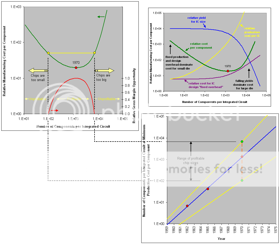
After years of fighting with Moore's Law, the industry will be finally be able to outpace it.

Moore's law is about the minimum point on the cost-per-component production curve for a given process node.

Graph1.png


You optimize for an expected cost-per-component curve and hope to hit your projected volumes as production costs depend on production volumes to first-order (but volume is something you can't know in advance, since you can't predict the unpredictable).

Graph3.png


That is why nodes are not outright replaced when the newest one is released to production. Nodes get used for decades, they are supplemental to existing new nodes for the express purpose of making what would be unprofitable products become profitable.

Meanwhile you can't simply shift existing profitable chips to a new process node and have them continue to be profitable on the new node (see the far-left side of the curve above, if the shrunk chip is too small then it actually increases production costs).

TSMCRevenuebyNodeQ12012.png


Outpacing Moore's Law means outpacing the historic rate in the reduction of cost-per-component itself...something that is not going to happen unless transitions to larger and larger wafers somehow magically happens at a rate that is faster than the historical norm. (which is not happening, we are actually falling behind the trend)

large_diameter_img_02.jpg


(this is a fun link to read through)
 
Last edited:

CPUarchitect

Senior member
Jun 7, 2011
223
0
0
The problem is that you compare the GTX580(GF110) against the GTX680(GK104). GF110 was the Flagship Fermi chip when GK104 is not the Flagship Kepler chip.

...

Now we pay more for middle end GPUs but that is another story ;)
No, it's definitely a huge part of the story. Do you honestly consider GK104 a mid-end GPU when the cards cost 499 bucks? GF104 (GTX 460) was launched at 199 and 229 MSRP for the 768 MB and 1024 MB version respectively: NVIDIA’s GeForce GTX 460: The $200 King.

And this just in: GK107 sucks at GPGPU as well.

So even if we assume that GK100/110 includes the dynamic scheduling they ripped out of Fermi, which I'm not challenging but is not guaranteed either, the conclusion is that the vast majority of Kepler parts that end up in consumer systems will be worse at GPGPU than the previous generation.

This is not something you can just ignore. And another salient point is that Apple is going with Kepler GPUs in all its new MacBook Air/Pro, iMac and Mac Pro systems, while Apple is the initiator of the OpenCL standard. So apparently they lost faith in GPGPU as well and don't want it to compromise graphics performance.
 

Riek

Senior member
Dec 16, 2008
409
15
76
This is not something you can just ignore. And another salient point is that Apple is going with Kepler GPUs in all its new MacBook Air/Pro, iMac and Mac Pro systems, while Apple is the initiator of the OpenCL standard. So apparently they lost faith in GPGPU as well and don't want it to compromise graphics performance.

But they will use IVB which also supports openCL.
 

CPUarchitect

Senior member
Jun 7, 2011
223
0
0
But they will use IVB which also supports openCL.
Sure, but with the CPU often being better at it than the GPU. And next year it's going to get way better at it with twice the throughput per core and gather support.

GPGPU is obviously on its decline. It didn't work out for discrete cards; NVIDIA wisely backed out. Now some are still clinging on to the hope that using a weak GPU that's closer to the CPU will fix it. But obviously the superior solution is to go one step further and bring GPU technology within the CPU cores. Homogeneous throughput computing will completely eradicate all the difficulties encountered with heterogeneous computing.
 

Dresdenboy

Golden Member
Jul 28, 2003
1,730
554
136
citavia.blog.de
Sure, but with the CPU often being better at it than the GPU. And next year it's going to get way better at it with twice the throughput per core and gather support.

GPGPU is obviously on its decline. It didn't work out for discrete cards; NVIDIA wisely backed out. Now some are still clinging on to the hope that using a weak GPU that's closer to the CPU will fix it. But obviously the superior solution is to go one step further and bring GPU technology within the CPU cores. Homogeneous throughput computing will completely eradicate all the difficulties encountered with heterogeneous computing.
Your hypothesis sounds very interesting. Do you have some numbers to back it up? I'd like to see if an AVX2 CPU is faster at different typical parallel compute tasks than a compute optimized GPU (like GK110) at the same power and a comparable process node.
 

Phynaz

Lifer
Mar 13, 2006
10,140
819
126
Why don't you start one? Why does it have to be "official" (whatever that is)?
 
Last edited:

piesquared

Golden Member
Oct 16, 2006
1,651
473
136
Well correct me if you're wrong, but don't I have to have mod status to move posts to a new thread?
 

Olikan

Platinum Member
Sep 23, 2011
2,023
275
126

piesquared

Golden Member
Oct 16, 2006
1,651
473
136
Are you refering to this paragraph?

After the show, a source confirmed that Kaveri will be a true Southern Islands GCN part in the GPU department, without any remnants of the HD6XXX VLIW-4 architecture, and that the Steamroller CPU core parts there would solve a couple of remaining major drawbacks of the Piledriver architecture.

I think what he means is that Kaveri will have full GCN (+HSA compliant features) as apposed to Trinity being VLIW4.
 
Status
Not open for further replies.