cdimauro
Member
- Sep 14, 2016
- 163
- 14
- 91
I know it, but I wanted that Abwx, the Zen expert, to tell it.Purple box in the image you posted: 2 load + 1 store per cycle
")

I know it, but I wanted that Abwx, the Zen expert, to tell it.Purple box in the image you posted: 2 load + 1 store per cycle
Why you've reported this slide? The correct one is another.
Anyway, I saw: the micro-op queue is able to take uops both from the decoder and the micro-op cache.
However it can only dispatch 6 uops/cycle, not 10, to the schedulers:
And BTW, you haven't answered to my question: where are located the L/S units?

I know it, but I wanted that Abwx, the Zen expert, to tell it.
But Intel has 4 ports which take care of store address operations, data loads and store, whereas on Zen you have to pass through the only 2 AGUs for it.
That's a consistent difference, especially for the FPU code.
Are you talking about Zen? Because Intel processors can do two instructions-fusion operations per cycle.
I edited my post and added the decode stage, there s 10 uops that can be dispatched simultaneously, 6 to the INT schedulers and 4 to the FP schedulers, if there s 10 uops available in the uop queue it doesnt make sense to pretend that only 6 can be dispatched, it s 6 only if the queued uops are all to be executed by the ALUs and none related to FP exe...
That was a useless question, but if it please you to make some smoke screen, well, you posted a slide that contradict your previous saying about Zen L/S being half of intel s CPU, one has to wonder if you did even bother to read some article here or there about Zen...
Btw, the diagram you posted is higher level than the ones i posted, of course using those high level slides allow to ignore the datas that are on the low level diagrams, we can see on the latter that the INT and FP dispatch use two different paths, wich render moot your "argmentation" that only 6 uops can be dispatched..
There are TWO slides which show that the micro-op queue dispatches 6 uops/cycle:I edited my post and added the decode stage, there s 10 uops that can be dispatched simultaneously, 6 to the INT schedulers and 4 to the FP schedulers, if there s 10 uops available in the uop queue it doesnt make sense to pretend that only 6 can be dispatched, it s 6 only if the queued uops are all to be executed by the ALUs and none related to FP exe...


I already explained that for using the L/S units you have to pass through the AGUs, which are ONLY TWO!That was a useless question, but if it please you to make some smoke screen, well, you posted a slide that contradict your previous saying about Zen L/S being half of intel s CPU, one has to wonder if you did even bother to read some article here or there about Zen...
See above: there are TWO slides which report the same information: 6 uops / cycle.Btw, the diagram you posted is higher level than the ones i posted, of course using those high level slides allow to ignore the datas that are on the low level diagrams, we can see on the latter that the INT and FP dispatch use two different paths, wich render moot your "argmentation" that only 6 uops can be dispatched..
There are TWO slides which show that the micro-op queue dispatches 6 uops/cycle:
I already explained that for using the L/S units you have to pass through the AGUs, which are ONLY TWO!
So you can execute 2 loads / cycle, or 1 load + 1 store / cycle, even if you have 2 loads + 1 store unit, because of the AGUs.
Understood?
There are TWO slides which show that the micro-op queue dispatches 6 uops/cycle:
See above: there are TWO slides which report the same information: 6 uops / cycle.
Trolling? Please, can you explain me how you can do it when you have to pass from the only TWO available AGUs?Are you trolling.?..
It s written 2 loads and 1 store per cycle on the very slide you posted, this has been already pointed by a member just a few posts before this one...
There are TWO slides which show that the micro-op queue dispatches 6 uops/cycle:
I already explained that for using the L/S units you have to pass through the AGUs, which are ONLY TWO!
So you can execute 2 loads / cycle, or 1 load + 1 store / cycle, even if you have 2 loads + 1 store unit, because of the AGUs.
Understood?
See above: there are TWO slides which report the same information: 6 uops / cycle.
Whatever are the memory operations, they all pass through the AGUs. See here:If the AGUs were a limit for the R/W ops, then i don't see the need of 3 ports on L1D. Probabily for simple addressing, like direct (e.g. [AX]), AGU is not needed... Also stack engine has his own AGUs.
In this article, we’ve provided a cursory review of the FO4 metric as it applies to the delay depth of a logic block. We also engaged in brief discussions using the barrel shifter as an example in illustrating the use of the FO4 metric. Finally, the barrel shifter also served as an example to illustrate that the FO4 depth of a logic block can be reduced through the use of more advanced circuits or better architectural re-arrangement of logic and arrays to minimize signal delay paths. What is not mentioned is that even more engineering resources may be applied to specific logic paths, especially if that logic path happens to be the critical path that limits the operating frequency of a processor. In a design that uses the standard cell libraries, the 2 input mux may itself be a standard cell, or smaller bit vector barrel shifters may be created as a standard cell with which larger bit vector shifters may be constructed from. Processors or ASICS that use standard cell design methodology require less design effort as compared with a full custom design effort. In a full custom design effort, logic circuits may be specifically tailored to a given process technology at the cost of engineering resources. This point is well covered in the article by Chinnery and Keutzer [3].
Physical implementation of a processor utilizing a full custom design methodology requires detailed simulations and considerations for a functional unit’s area, power, and latency. The optimal design point of each logic block would depend on the assumptions made in the overall microarchitecture of the processor. However, such detailed simulations and considerations are not needed in cases where a processor’s architects wish to perform preliminary research into a new and novel architecture. The FO4 metric provides an abstraction from physical circuit implementations and allows architects to project, design and simulate a processor without knowing the specifics and details of the implementation. As a result, the FO4 metric is useful and popular metric used by architects and engineers as a basis to explore architectural concepts at an abstract level.
Whatever are the memory operations, they all pass through the AGUs. See here:
And it's interesting to note that the AGUs can access just 1 Store Queue and 1 Load Queue. So, you're limited to 1 Load + 1 Store dispatched the proper queue, per cycle.
I don't know why it's reported 2 loads. Maybe there can be the possibility to "fuse" two loads which are made at consecutive memory locations, but this is just a speculation.
This is what i was referring to. I remember that article...Some info on the FO4 delay metric that people keep bringing up:
http://www.realworldtech.com/fo4-metric/5/
Stack operations have to deal with pushes (stores) and pops (loads) to/from the stack's memory, so you need load + store units, which doesn't match with the available information.I think that this is a simplified diagram. There is not even the stack engine depicted. They clearly stated that the stack engine has its own AGUs...
There is a sort of L0 cache (called memory file) and I think that "cache" miss are redirected to L1D cache and here the AGU calculation were already made... The stack engine is upper in the hierarchy and "steals" stack instructions from uop stream...Stack operations have to deal with pushes (stores) and pops (loads) to/from the stack's memory, so you need load + store units, which doesn't match with the available information.
But its operations go to the dispatcher. Take a look at the frontend slide.There is a sort of L0 cache (called memory file) and I think that "cache" miss are redirected to L1D cache and here the AGU calculation were already made... The stack engine is upper in the hierarchy and "steals" stack instructions from uop stream...

Well, the only thing that I think is that you can have hard times even with elementary fluid dynamics.And both slides show 6 uops dispatched to the INT unit, that s high level, the low level slide show 6 explicitely to the INT path.
According to Hardware.Fr the INT and FP part of the CP can work independently without a part stalling the other one, wich could happen in previous uarches.
As said it doesnt make sense that if there s more than 6 uops in the queue that only 6 could be dispatched since the FP path is separated, the limitation to 6 is if it s exclusively INT code, but you can of course think otherwise if that s somewhat relieving for you, after all better to make wrong assumptions than losing sleep, isnt it...
http://www.anandtech.com/show/10591...t-2-extracting-instructionlevel-parallelism/3The new Stack Engine comes into play between the queue and the dispatch, allowing for a low-power address generation when it is already known from previous cycles. This allows the system to save power from going through the AGU and cycling back around to the caches.
Finally, the dispatch can apply six instructions per cycle, at a maximum rate of 6/cycle to the INT scheduler or 4/cycle to the FP scheduler. We confirmed with AMD that the dispatch unit can simultaneously dispatch to both INT and FP inside the same cycle, which can maximize throughput (the alternative would be to alternate each cycle, which reduces efficiency). We are told that the operations used in Zen for the uOp cache are ‘pretty dense’, and equivalent to x86 operations in most cases.
I don't think dismissing a shipping game as an "outlier" is necessarily the best response. Why is Cinebench so vastly popular here? It's just one program. Why isn't it an outlier?An outlier of a game or two doesn't change the fact that most of the time BD and its derivatives just can't keep up.
One can get an 8320E and a board capable of clocking it at 4.4 GHz on air for $130 after rebate with tax at Micro Center. That is enough to meet the performance of the 9370, performance that can be adequate depending on the workload and how optimal the coding of the software is.Piledriver/Vishera was a fine CPU back in its day when competing with Sandy (8350 matching 2500k as expected)... nowadays it's game over.
They're stupid parts because they use turbo, which is not at all optimal. The Stilt also says the leakage is worse with those than with the E chips. It makes more sense to get a cheaper 8 core FX and overclock it. Even the plain 8320 has shown fine results from what I've read.The 9370 and 9590 are that high in the charts through balls to the wall overclocking and overvolting for an off the shelf consumer part.
I think the reasons AMD didn't improve upon Piledriver for the enthusiast and server arenas is because of its weakened market position thanks to Intel's tactics (as well as its various managerial errors over the years) and the decision that it would try to have stronger sales of Zen by withholding an upgrade, making Zen seem better. This latter decision seems to be due to the limitations of node improvement from GoFlo since 32nm SOI. I'm speculating but it seems sensible that, if AMD can't offer Skylake or Kaby performance with Zen it can, at least, point to a vast improvement over Piledriver (thanks to Piledriver's old age).in XV the low hanging fruit in the design has been picked and further refinement could do wonders, as you say. BR as it is, a cache starved part on an outdated 28nm process tuned for sheer density, is a much stronger product than Trinity/Richland were. Imagine what a four module XV v2 part with L3 and a better uncore could do as replacement for Vishera, designed for higher power on a newer, better node... sadly we won't get to see that. Another what if.
AMD knows very well why they didn't keep pursuing the BD lineage for high performance and power usage, instead decided to design a new core. Zen should be more all around more competitive than BD ever was in any of its iterations given the 40% figure over XV... if it can clock high enough.
Then there should be some misleading information in the slides. Let me quickly recap.cdimauro, that's the sustained vs. peak story again.
How about this:
http://www.anandtech.com/show/10591...t-2-extracting-instructionlevel-parallelism/3
And let me point you at the differences between AMD's "instructions", "micro-ops" and "µops" (the latter as found in the schedulers). According to Mike Clark, those "dense" micro ops get split up in the dispatch unit. This should include "fast path doubles" like 256b AVX ops. Those instructions fused by a micro-op fusion in Intel CPUs usually covers EX+mem ops (IIRC since Banias). That type of instructions gets decoded as one Cop/Mop/instruction in AMD's processors (no splitting up in the first place). Macro-op fusion (test+branch) is the only fusion happening in AMD's chips. Whether the "fast path doubles" (med complex x86 ops which break up into up to 4 uops later, e.g. 256b avx + mem) can be decoded at a rate of 4/cycle remains to be seen, as it was different in the past.
A lot of information can be found in the GCC patches both for Intel's and AMD's x86 processors, including latencies, throughput (in most cases), dependencies, unit occupancy, etc.
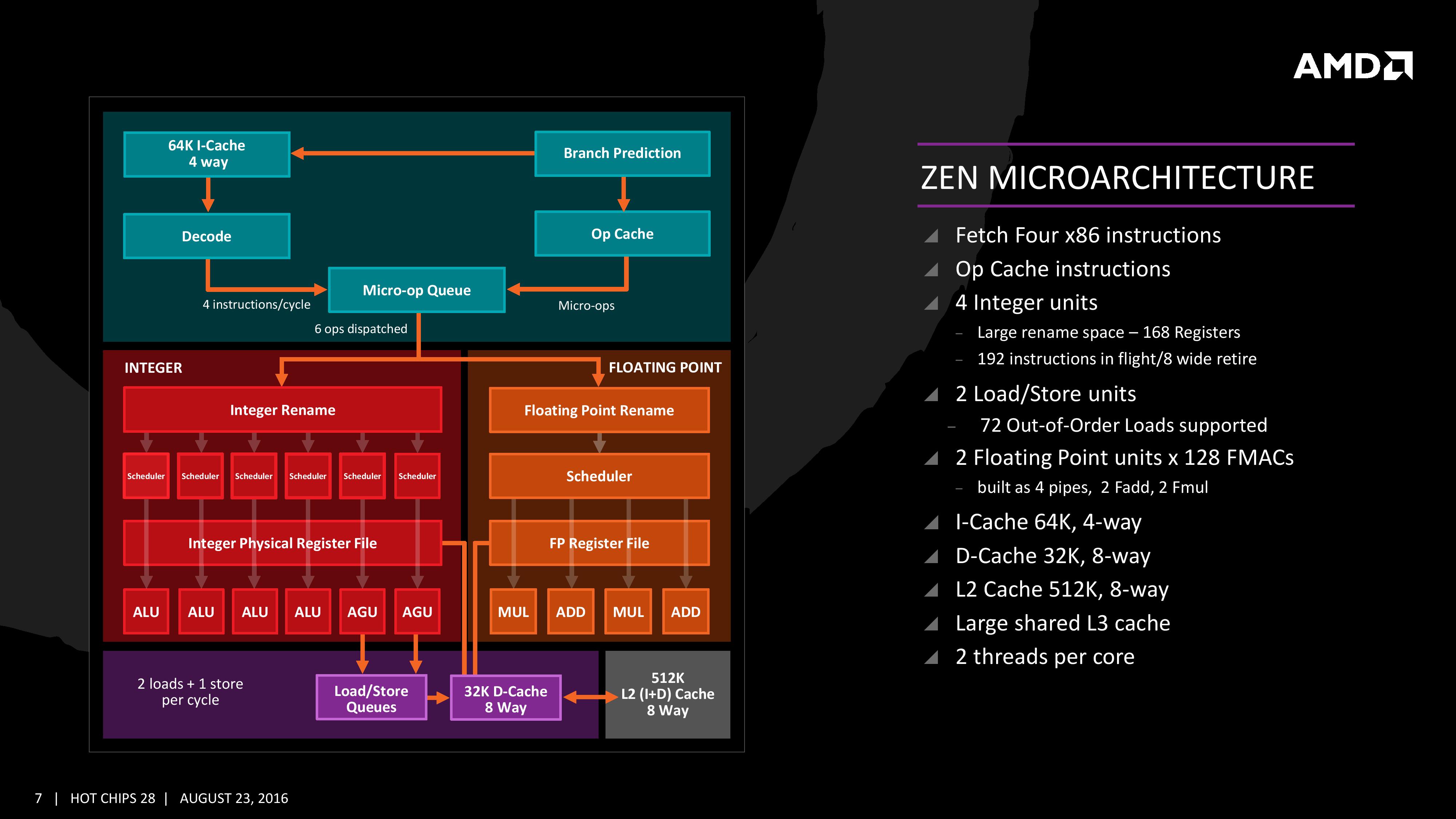


Then there should be some misleading information in the slides. Let me quickly recap.
According to these two slides:
The Micro-op Queue receives micro-ops (obviously) from the Decoder and the Op-Cache, but then dispatches 6 uops (NOT micro-ops!).
Whereas in this slide:
the dispatcher sends Micro-ops (6 + 4), which shouldn't be the case.
En pratique 10 micro ops peuvent être envoyées (6 vers la partie "Integer" de la puce, 4 vers la partie "Floating Point"), soit deux de plus que sur Haswell (Intel ne nous a pas donné l'information pour Skylake).
No this is 100% wrong, there are load and store QUEUE's after the AGU's. You can issue 2 load and a store a cycle as clearly said by michael clark @ 12:39 into the hot chips presentation.I already explained that for using the L/S units you have to pass through the AGUs, which are ONLY TWO!
So you can execute 2 loads / cycle, or 1 load + 1 store / cycle, even if you have 2 loads + 1 store unit, because of the AGUs.
Understood?
See above: there are TWO slides which report the same information: 6 uops / cycle.
No this is 100% wrong, there are load and store QUEUE's after the AGU's. You can issue 2 load and a store a cycle as clearly said by michael clark @ 12:39 into the hot chips presentation.
You are also completely ignoring the stack engine ( which is used to do address gen + unknown stuff for stack address/data).
Also you keep saying Intel has 4 L/S ports, they do not, they have dedicated store AGU ( does not move data!) a dedicated store port (doesn't generate addresses!) and two generate purpose AGU's that can each do a load. So aggregate is 3!
So the question is on average what percentage of loads are for the stack, because AMD doesn't use the AGU to calc its address, so its completely plausible that >haswell and Zen issue on average the same amount of loads and stores a cycle.
This setup looks similar to the K12 one, just that the latter has one more AGU to feed the queues.But its operations go to the dispatcher. Take a look at the frontend slide.
Anyway, the solution is in another slide:
Both AGUs can send operations to the Load or Store Queue, and the Load Queue can do two loads.
Anyway, and as I've already stated, you have only 2 AGUs, so you can only dispatch 2 memory operations per cycle to the proper queue.
) can even contain a RMW op, this should save one AGU issue slot. OTOH these instructions just make up some lowish percent (3%?) of all ops. That discussion took place at SemiAccurate a while back.