AMD Ryzen (Summit Ridge) Benchmarks Thread (use new thread)

Page 40 - Seeking answers? Join the AnandTech community: where nearly half-a-million members share solutions and discuss the latest tech.
Status
Not open for further replies.

TheELF

Diamond Member
Dec 22, 2012
4,027
753
126
How come the Zen ES @3GHz not melted then, but draw less power than a 3GHz clocked BW-E?
Because 16 low speed cores draw lees power then 8 high speed cores with HTT?

  • 40% more instructions per cycle says nothing about how fast these instructions get executed
  • every AMD module until now shows up as one core with two (CMT) threads the fact that they changed Clustered with Symmetrical only tells us that every thread will have access to the same amount of resources.It's not HTT.
 

bjt2

Senior member
Sep 11, 2016
784
180
86
It's extremely difficult to select multiple uops from a single queue in a single cycle at a high (let's say > 2 GHz) frequency.

As far as I know only Intel is using a unified scheduler. I guess that part of their design is tuned at the transistor level. But I wonder if they still use a fully unified scheduler, or if it's internally splitting the queue.

This is very difficult with multiple issue scheduler. But in an one lane scheduler, this is the only job it has to do: select among a few in the queue (maybe even taking into account thread priority, a new feature of Zen's SMT), from ready intruction, taking into account the final timing of the currently executing instruction (e.g. if it's a MUL it does not have one cycle latency). Modern CPUs are OOO. Even in a one queue/one pipelin configuration a choiche must be made...

Regarding INTEL... The unified scheduler is IMHO the one thing that keep clocks down... So they tuned the rest of the pipeline to have less stages, keeping in mind that the clock limit probabily is given by the scheduler... It seems that INTEL CPUs hit a wall in OC even if the consumption is not so high... I doubt that is the caches, decoder or calculation units... I think it's the unified scheduler...
 

bjt2

Senior member
Sep 11, 2016
784
180
86
Because 16 low speed cores draw lees power then 8 high speed cores with HTT?

  • 40% more instructions per cycle says nothing about how fast these instructions get executed
  • every AMD module until now shows up as one core with two (CMT) threads the fact that they changed Clustered with Symmetrical only tells us that every thread will have access to the same amount of resources.It's not HTT.

Zen ES was 8 cores 16 thread, like the Broadwell-E used for comparison. It drawn less power than the BWE with the same software. BW-E is clocked at 3.2GHz at default, with an higher all-core turbo in 128-bit mode. Zen was an ES. And still there is someone who can't admit that Zen will be clocked more than 3GHz?!?!?!
 

Abwx

Lifer
Apr 2, 2011
11,885
4,873
136
We just have no info on what the ZEN core will be like,we DO know what the Broadwell core is like.

We have all the necessary infos, besides AMD gives way more infos than Intel has ever given, including for BDW, find us something comparable from Intel, particularly the slide about SMT...

AMD-Zen_Microarchitecture.png


amd-zen-le-recap-12.jpg


Now if thoses diagrams are of no help to you why even trying to discuss how it will perform or not..?.
 

bjt2

Senior member
Sep 11, 2016
784
180
86
The FX-8xxx is also 4 cores 8 threads...
We just have no info on what the ZEN core will be like,we DO know what the Broadwell core is like.

Are you kidding? It was official statement that the Zen ES that was tested versus Broadwell-E was an 8 core 16 thread part, that there will be a 4 core 8 thread and 8 core and 16 thread at launch...
 

The Stilt

Golden Member
Dec 5, 2015
1,709
3,057
106
So my question's answer is: It's your opinion and not inside knowledge. That's fine. I needed clarification as I didn't know if you had developed some cues by testing of any Zen samples.

Your question I'll answer: Sure, it can have a limit and can be a limiter. But I don't believe, as you stated that you do, that L2 is what will limit Zens frequency... Not until ~4GHz I don't anyway. If the FO4 is similar, it is possible for Zen to be hitting XV (and even Deneb) speeds, by design. Also,

Firstly, SRAM in seclusion is generally easiest to clock high at low volts. Hence why every new process is shown off using these. Intels 14nm bitcells were hitting 1.5GHz at 0.6V. However, the type of SRAM (4 MOSFET vs 6 or 7 or 8) will make a difference.

Secondly, I don't know if Zen will hit 3.2-3.8GHz within 9 months, or not, and I'm really not sure if 3.2-3.4GHz will launch. Indications are negative but they have delayed for a reason that would be substantial. I really don't know how good the process is, nor the design or the process learning curve/maturity level. Timing bugs and lower performing process are entirely possible at this stage of a new m.arch+new process. So far, all indications point to low clocks, combined with the LPP historical data, but why that is, and if they can be improved with tuning and maturity, and how quickly, remains to be seen.

Agena clocked piss poor Brisbane style. Deneb clocked awesome, hitting 3.7GHz at lower power. Same low pipeline stage design, FO4 design.

Lastly, yes, cache occupies a large chunk of delay in the processors cycle-limiting paths. Hence why I don't disregard it as a factor. I don't however believe it will be the most critical factor at play.

Sent from HTC 10
(Opinions are own)

Yes, Zeppelin is another of the two designs I won't be testing in advance, or at all. The other one was the initial 10h model(s).

Also, I don't think it would be unreasonable to speculate if Zen might have similar issues as all of the past designs have had. Zen is drastically different if compared to 15h or 10h, however so are 15h and 10h. Yet the same exact behavior can seen on both of them.
Regarding the actual difference between the cores and the L2 Fmax on 15h (Piledriver), up to 800MHz or 200mV is not unheard of. The cache scales well with the voltage, however because the voltage must be increased extremely rapidly the design soon becomes limited by the thermals and / or the power delivery. Pushing Piledriver beyond ~ 4GHz is a huge waste of power. That's because the power distribution (within a full core, i.e core + L2) is around 9:1 (cores, L2 cache). So when you are feeding up to 200mV higher voltage to the cores than they actually need... That's exactly why the highest clocked Piledrivers have TDP of 220W.

Likewise with high clock capable GCN ASICs (such as Bonaire), once you hit the frequency limit you can adjust the L2 cache clock speed in relation to the core / ROPs. The standard setting is 1/1 for all GCN ASICs, but you can configure it down to 1/4 if necessary. 3/4 setting usually will allow you to go up to the process limits. This has no effect at all or a perfectly linear effect to the performance, depending on workload. No CPU that I know of has an adjustable L2 ratio.

Also I think there was a reason why Bobcat (14h) had it's L2 caches running at 1/2 rate. Could have been due the manufacturing process (TSMC 40nm) or due some other factor, but I don't think it was due the power consumption.
 

Nothingness

Diamond Member
Jul 3, 2013
3,307
2,379
136
This is very difficult with multiple issue scheduler. But in an one lane scheduler, this is the only job it has to do: select among a few in the queue (maybe even taking into account thread priority, a new feature of Zen's SMT), from ready intruction, taking into account the final timing of the currently executing instruction (e.g. if it's a MUL it does not have one cycle latency). Modern CPUs are OOO. Even in a one queue/one pipelin configuration a choiche must be made...

Regarding INTEL... The unified scheduler is IMHO the one thing that keep clocks down... So they tuned the rest of the pipeline to have less stages, keeping in mind that the clock limit probabily is given by the scheduler... It seems that INTEL CPUs hit a wall in OC even if the consumption is not so high... I doubt that is the caches, decoder or calculation units... I think it's the unified scheduler...
Sorry, but you are wrong :)

As an exercise try to pick three "good" instructions from a single issue queue. What algorithm do you pick? Is it hard to pick the 3 oldest instructions in your queue? Now compare this to picking the oldest instruction from 3 queues. Which one will provide you with the highest clock?

Note I'm not talking about getting the best scheduling (which anyway requires to know the future), but about reaching high enough clocks. Splitting instructions into multiple queues will have an impact on scheduling, but the impact is lower than the one required to issue multiple instructions from a single queue (unless you're named Intel :D).
 

bjt2

Senior member
Sep 11, 2016
784
180
86
Sorry, but you are wrong :)

As an exercise try to pick three "good" instructions from a single issue queue. What algorithm do you pick? Is it hard to pick the 3 oldest instructions in your queue? Now compare this to picking the oldest instruction from 3 queues. Which one will provide you with the highest clock?

Note I'm not talking about getting the best scheduling (which anyway requires to know the future), but about reaching high enough clocks. Splitting instructions into multiple queues will have an impact on scheduling, but the impact is lower than the one required to issue multiple instructions from a single queue (unless you're named Intel :D).

Maybe I misunderstood, but this is exactly what I said: 6 split queues for each of the 6 units can give faster clocks with a small IPC penality: AMD is specialized in this since K7-K10 was similar with no jump between queues, albeit with coupled ALU+AGU...

And two fat queue or worse one fatter queue maybe help a little with the IPC, but gives slower clocks and higher consumption...

Maybe AMD uses split queues more for low power consumption than for higher clocks...
 
Last edited:

Nothingness

Diamond Member
Jul 3, 2013
3,307
2,379
136
Maybe I misunderstood, but this is exactly what I said: 6 split queues for each of the 6 units can give faster clocks with a small IPC penality: AMD is specialized in this since K7-K10 was similar with no jump between queues, albeit with coupled ALU+AGU...

And two fat queue or worse one fatter queue maybe help a little with the IPC, but gives slower clocks and higher consumption...

Maybe AMD uses split queues more for low power consumption than for higher clocks...
I misunderstood your previous post, so we agree :)
 

itsmydamnation

Diamond Member
Feb 6, 2011
3,076
3,908
136
Maybe I misunderstood, but this is exactly what I said: 6 split queues for each of the 6 units can give faster clocks with a small IPC penality: AMD is specialized in this since K7-K10 was similar with no jump between queues, albeit with coupled ALU+AGU...

And two fat queue or worse one fatter queue maybe help a little with the IPC, but gives slower clocks and higher consumption...

Maybe AMD uses split queues more for low power consumption than for higher clocks...
The diagrams show a forwarding network between the queue's and ALU/AGU. So that would say that schedulers should be able to send to a set/any ALU/AGU (otherwise why include it), maybe with a forwarding penalty etc? I think there is significantly more complexity here then AMD is talking about.

As speculated by Dresdenboy maybe this is just a method to allow for opportunistic in order scheduling ( amd have papers for this). By having many smaller queues you can process each of them in order at the same time and then if a queue can't issue in order it uses the more expensive OOO components of the schedulers.

This queuing idea is pretty common for example in almost all highend network hardware there are many ( 8-10) shallow queue's that internally are process FIFO.

But its all the stuff they haven't shown on the diagram that will determine how this setup actually works. I would expect for example some type of scheduler of schedulers that's making intelligent decisions on which scheduler to forward the op to. For the speculated in order to work well you would think a scheduler must be able to issue any type of operation, from memory Zen has at minimum 2x of every function so maybe execution units are arranged in two 2ALU+1AGLU clusters or something like that to simplify muxes/forwarding.

AMD have done a good job of showing there is plenty of performance potential without showing how anything actually works :)
 

bjt2

Senior member
Sep 11, 2016
784
180
86
The diagrams show a forwarding network between the queue's and ALU/AGU. So that would say that schedulers should be able to send to a set/any ALU/AGU (otherwise why include it), maybe with a forwarding penalty etc? I think there is significantly more complexity here then AMD is talking about.

As speculated by Dresdenboy maybe this is just a method to allow for opportunistic in order scheduling ( amd have papers for this). By having many smaller queues you can process each of them in order at the same time and then if a queue can't issue in order it uses the more expensive OOO components of the schedulers.

This queuing idea is pretty common for example in almost all highend network hardware there are many ( 8-10) shallow queue's that internally are process FIFO.

But its all the stuff they haven't shown on the diagram that will determine how this setup actually works. I would expect for example some type of scheduler of schedulers that's making intelligent decisions on which scheduler to forward the op to. For the speculated in order to work well you would think a scheduler must be able to issue any type of operation, from memory Zen has at minimum 2x of every function so maybe execution units are arranged in two 2ALU+1AGLU clusters or something like that to simplify muxes/forwarding.

AMD have done a good job of showing there is plenty of performance potential without showing how anything actually works :)

Interesting... You mean this image? At first I thought that the gray lines were there only to retire the ALU and optional AGU operation together, because to have lane switching each lane should be connected to the other and the diagram seems imply only ALU->AGU connenction... The other thing of dinamic OOO/in-order switching is very interesting, at least in terms of power consumption (and thus maximum clock)

HC28.AMD.Mike%20Clark.final-page-010.jpg


All in Zen seems to be here to have minimum power consumption. I don't see why this should not take to higher clock...
 

itsmydamnation

Diamond Member
Feb 6, 2011
3,076
3,908
136
yeah im just spit balling and the problem with these diagrams can be if they are drawn to reality you can just end up with a mess of arrows.
 

cbn

Lifer
Mar 27, 2009
12,968
221
106
Looking at the die shot of Summit Ridge below, I wonder if AMD could use chop lines (and a new mask set) to create a new smaller quad core die? This using the bottom half of the die.

It would only have single channel memory though, but if it is actually feasible it would be a way to the increase the pool of 4C/8T and 3C/6T Zen for the ever improving range of mid-level and better dGPUs.

LL
 

cdimauro

Member
Sep 14, 2016
163
14
91
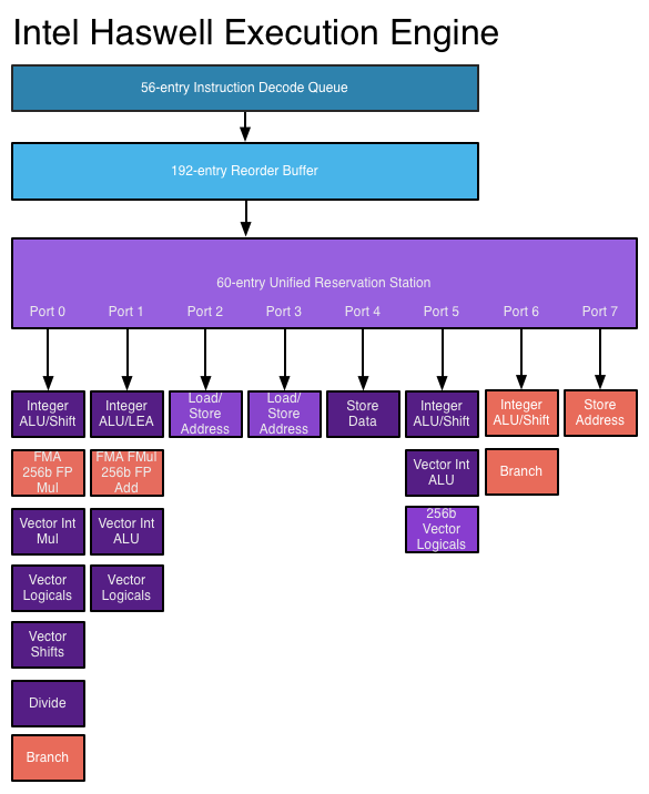
Taking a look at posted diagrams and at Haswell's one (Broadwell has the same):
haswellexec.png

and to quickly recap, I don't see so much differences between the two approaches.

In Zen, the complexity of selecting the proper instructions to dispatch (and execute) to some schedulers is moved into the so called "Rename" ("Map" in the last slide) stage/units.

After that only the 4 Integer schedulers seems (again, last slide) to have some capability to put instructions to the Retire unit. It might be that AMD resolves / eliminates / executes the registers "move" instructions into this stage, avoiding to continue the execution and wasting an ALU for this. In fact, you already did the registers renaming, and at this point you can commit (retire) the instruction. Pay attention that AGUs aren't affected by this (look at the diagram): only integer instructions are.

But except for this, and as I've written, before that you need to properly schedule the instructions to execute, and putting them on the proper execution unit (through the proper single scheduler, which I think takes care to check if all arguments/resources of the instructions are there before executing it).

This is more or less what Haswell does (see the diagram), except that with Zen there's an additional step to dispatch an instruction to the Integer/AGU or FPU Rename unit.

I don't take into account the different instruction latencies, because both integer and FPU instructions have very different (and sometimes huge) ones to take care of. In short: an integer scheduler has complex stuff to handle, as well an FPU one. And in the x86 world, both have to care of micro-coded instructions.

To finalize, I think that selecting an instruction and putting it into the proper scheduler or execution port (with 6 schedulers or 8 ports to select requires a 3-inputs MUX anyway) is a very similar task for both approaches which involves more or less the same complexity and impacts as well the reached frequencies (IF this is the real bottleneck for the final clock).
 

bjt2

Senior member
Sep 11, 2016
784
180
86
The "problem" in core CPUs is that the scheduler is unified, so it must handle all the instruction type, with all combinations. Most notably INT and FP, with latencies ranging from 1 to few cycles (we are talking of uops). More combination means more complex decoding, more transistors, more layers, more FO4, more consumption. Even if the complexity lies in the MAP stage, in Zen, it must handle only INTEGER instruction. Less combination, less conflicts (i imagine the nightmare of scheduling conflicting int and fp uops and deciding the best port in core CPUs), less tranistors, less FO4, less power consumption...
 

cdimauro

Member
Sep 14, 2016
163
14
91
I'm not an expert in microarchitectures, but I don't think so, and let me quickly explain why.

At that stage, you don't have to decode anything: you only have to send a uop in a proper port/execution unit, for the concrete execution. If the uop is INT or FP, it doesn't matter; it doesn't matter also about its latency.

Probably the uop has coded inside a set of ports where it can be executed (as well as which the resources, if any, are needed). The scheduler has "just" to select one of such ports which is free at the time (and with the needed resources which are available; like an operand coming from memory). That's it.

Of course, the less are the ports, the less are the checks to be made for picking one.

However pay attention about another thing: some INT instructions require access to FP registers, or viceversa. There aren't many, but some of them are used (and are useful) for copying/converting values between the two different "macro-areas". Handling this with a unified scheduler is a piece of cake: just ordinary administration. But it's a black beast with separated INT and FP schedulers...

There's also nothing which is known or shows that it's the scheduler which defines the FO4 of a pipeline, and that influences consistently the power consumption and/or the transistors budget. On the contrary, I think that having so many separated resources (rename units, schedulers, queues) can contribute for the opposite.

Last but not least and as I already said, Zen seems to need an additional stage from the uop cache to deliver the uops to the proper "macro-area" (INT or FP scheduler). And then you have both the need to dispatch the uop to one of the 6 "schedulers" (3-inputs MUX), and in parallel the unified uop scheduler has to handle the coming uops.
 

Nothingness

Diamond Member
Jul 3, 2013
3,307
2,379
136
I'm not an expert in microarchitectures, but I don't think so, and let me quickly explain why.

At that stage, you don't have to decode anything: you only have to send a uop in a proper port/execution unit, for the concrete execution. If the uop is INT or FP, it doesn't matter; it doesn't matter also about its latency.

Probably the uop has coded inside a set of ports where it can be executed (as well as which the resources, if any, are needed). The scheduler has "just" to select one of such ports which is free at the time (and with the needed resources which are available; like an operand coming from memory). That's it.

Of course, the less are the ports, the less are the checks to be made for picking one.
That's much more complex than that. Instructions stand in a queue until their dependencies are resolved, which happens OoO. This means instructions get ready OoO. The simplest good working scheduling algorithm is the one that picks the oldest instruction. Now imagine the work needed to pick the two oldest instructions.

A classic article from Intel about scheduling is Matrix Scheduler Reloaded. Quite gory :D
 

Phynaz

Lifer
Mar 13, 2006
10,140
819
126
Instructions stand in a queue until their dependencies are resolved, which happens OoO. This means instructions get ready OoO.

I believe I read that once instructions get to the Reservation Station they are in-order at that point. Remember they are no longer x86 at this point, and they got placed in the correct execution order in the prior block - the Reorder Buffer.
 

cdimauro

Member
Sep 14, 2016
163
14
91
Correct. I was referring to the Unified Reservation Station (of Intel CPUs), which has to dispatch uops to the proper ports.
 
Mar 10, 2006
11,715
2,012
126
That's much more complex than that. Instructions stand in a queue until their dependencies are resolved, which happens OoO. This means instructions get ready OoO. The simplest good working scheduling algorithm is the one that picks the oldest instruction. Now imagine the work needed to pick the two oldest instructions.

A classic article from Intel about scheduling is Matrix Scheduler Reloaded. Quite gory :D

So is the bottom line here that running a unified scheduler at high frequencies is tougher to implement than separate Int/FP schedulers at high frequency?
 

Nothingness

Diamond Member
Jul 3, 2013
3,307
2,379
136
So is the bottom line here that running a unified scheduler at high frequencies is tougher to implement than separate Int/FP schedulers at high frequency?
Definitely, yes. A unified scheduler helps getting better schedules, but I'm not sure it's worth the price, unless you have time and people to tune at the transistor level.
 

bjt2

Senior member
Sep 11, 2016
784
180
86
I'm not an expert in microarchitectures, but I don't think so, and let me quickly explain why.

At that stage, you don't have to decode anything: you only have to send a uop in a proper port/execution unit, for the concrete execution. If the uop is INT or FP, it doesn't matter; it doesn't matter also about its latency.

Probably the uop has coded inside a set of ports where it can be executed (as well as which the resources, if any, are needed). The scheduler has "just" to select one of such ports which is free at the time (and with the needed resources which are available; like an operand coming from memory). That's it.

Of course, the less are the ports, the less are the checks to be made for picking one.

However pay attention about another thing: some INT instructions require access to FP registers, or viceversa. There aren't many, but some of them are used (and are useful) for copying/converting values between the two different "macro-areas". Handling this with a unified scheduler is a piece of cake: just ordinary administration. But it's a black beast with separated INT and FP schedulers...

There's also nothing which is known or shows that it's the scheduler which defines the FO4 of a pipeline, and that influences consistently the power consumption and/or the transistors budget. On the contrary, I think that having so many separated resources (rename units, schedulers, queues) can contribute for the opposite.

Last but not least and as I already said, Zen seems to need an additional stage from the uop cache to deliver the uops to the proper "macro-area" (INT or FP scheduler). And then you have both the need to dispatch the uop to one of the 6 "schedulers" (3-inputs MUX), and in parallel the unified uop scheduler has to handle the coming uops.

The possible combinations, and the required logic, grows with the factiorial (n!), so it's useful to split into domain. Power 8 and 9 have more domains: int, branch, memory and FP (and maybe i forgot something). But yes this comes at one price: longer latencies on intructions that move data between domains... I don0t think that they are more than a few percent of the executed instructions...

With Zen you also need to dispatch the uops to the proper "schedulers". ;)

This is a simple scheduling. Actually can also be a single bit in the uop, that can be set by the decoders...
 
Status
Not open for further replies.