Question AMD Phoenix/Zen 4 APU Speculation and Discussion

Page 11 - Seeking answers? Join the AnandTech community: where nearly half-a-million members share solutions and discuss the latest tech.

DisEnchantment

Golden Member
Mar 3, 2017
1,604
5,793
136
It's called DirectML and it's been around for a while as a part of DX12.
It cannot be DirectML, this would treat the AIE engine just like another SIMD capable device with mixed precision and/or matrix operations support.
The AIE graph compiler would need model/network information in order to lay out the layers/parameters/activation functions across the different tiles of the AIE PIM blocks.
Therefore WinML is more suitable.


If you are developing on Visual Studio, there are NuGet packages to use and import already trained ONNX models directly, for inferencing within an app. It is fairly easy I would say.
MS is fairly active on WinML in GitHub and you can see devblogs articles regularly on the topic.

Intel Movidus already have WinML support

I think it's up to AMD to make sure that their AI acceleration hardware (AIE or otherwise) is compliant with existing APIs/programming toolchains. If someone has an inference workload, they're going to target an API, not a specific logic block.
Indeed, they already stated it will be WinML, which makes sense, as stated above.


Also mentioned by Victor is that it is for inferencing mainly and will support only Ryzen processors with AIE and likely fallback to CPU if no AIE.

1655187259496.png

Of course WinML can use GPUs too, but the at the cost of efficiency but devs would probably have to take a call and AMD is limiting its WinML support to Ryzen CPUs, see fine print.

The framework exist, how pervasive it gets on Windows ecosystem remains to be seen.
 
Last edited:

uzzi38

Platinum Member
Oct 16, 2019
2,632
5,958
146
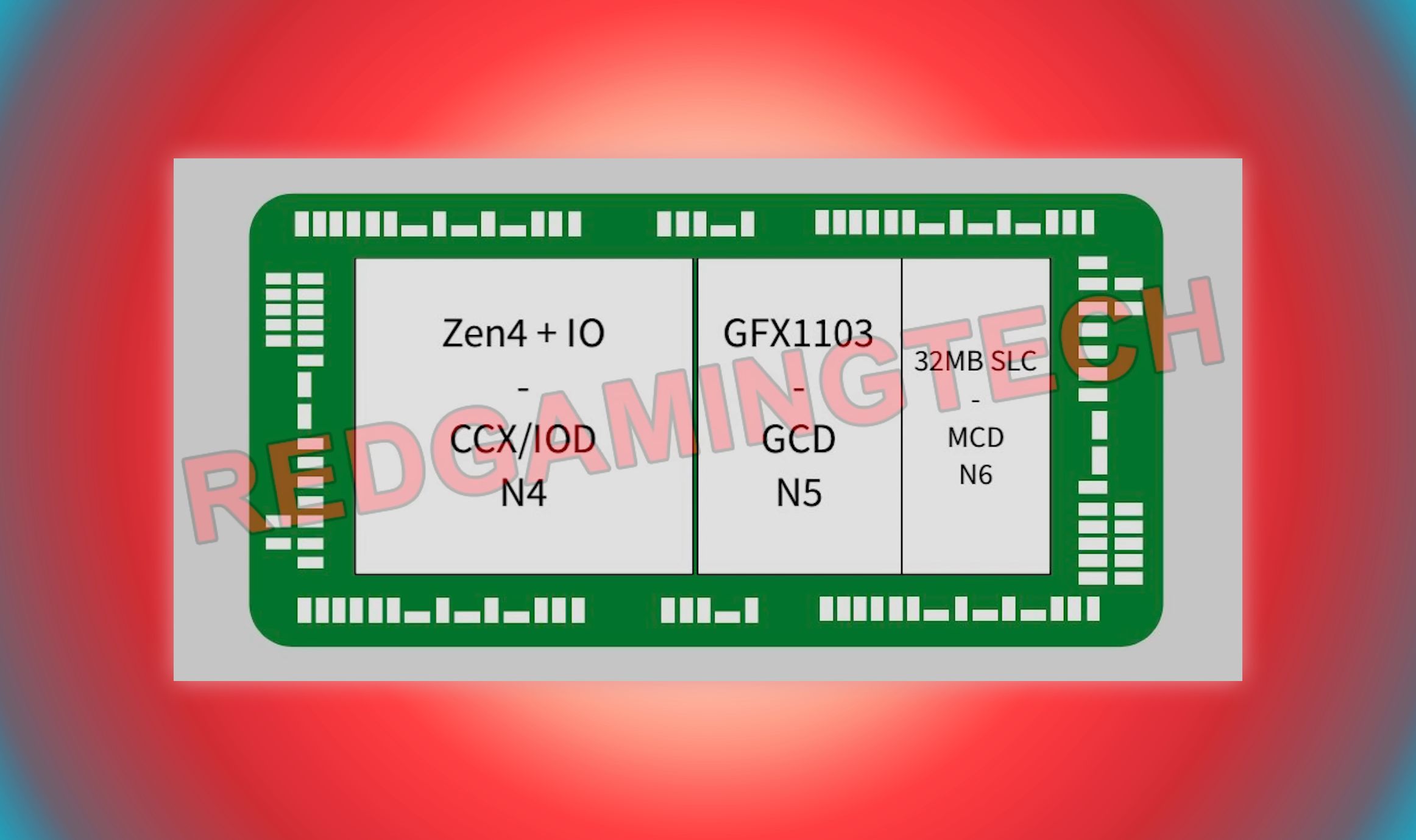
Indeed, I am wondering what AMD really meant with that statement that Phoenix is using chiplet architecture.
Not sure if it is something they will do but cache chiplet will bring tangible improvements in graphics which can be perceived by users immediately.

If there is some infinity cache, with 12CUs @~2.5 GHz it would be beyond RX470 level in TF and considering the gen on gen gains that would be some capable GPU in a thin notebook.
They can remove that chiplet for business laptops.
Phoenix looks like its going to be a great chip, very well balanced.
The N4 should help bring that TDP back to 15W or less for many SKUs and improving sustained performance. Should greatly help x86 efficiency standing in mobile.

In the end the bean counters will decide probably.
The whole chiplet archtecture thing has taken me by surprise. I hadn't heard anything about Phoenix being chiplet based at all, and tbh I still don't really believe it. But I mean, I'm more than happy to be wrong hahaha.
 

GodisanAtheist

Diamond Member
Nov 16, 2006
6,814
7,170
136
I hope that we see some of this make the hop to consumer space. HBM on an APU would be insane, and I think a unified SLC would also be what would really let consumer APUs punch above their weight.

- I think IC chiplets will provide the biggest bang for the buck for APUs, and likely where AMD will go next.

HBM has to be sourced from an external vendor while IC chiplets will already be manufactured en masse by TSMC for AMD for use in a wide variety of their products.
 

moinmoin

Diamond Member
Jun 1, 2017
4,952
7,661
136
The whole chiplet archtecture thing has taken me by surprise. I hadn't heard anything about Phoenix being chiplet based at all, and tbh I still don't really believe it. But I mean, I'm more than happy to be wrong hahaha.
Technically there is still the possibility Phoenix Point (btw. when and why was the "Point" part added?) is effectively monolithic and using "AMD chiplet architecture" without really being chiplets based, like e.g. an otherwise monolithic die containing the standardized chiplet interface UCIe to connect an external Xilinx AIE die or whatever. But with that mention AMD definitively raised expectations.
 

Mopetar

Diamond Member
Jan 31, 2011
7,837
5,992
136
- I think IC chiplets will provide the biggest bang for the buck for APUs, and likely where AMD will go next.

HBM has to be sourced from an external vendor while IC chiplets will already be manufactured en masse by TSMC for AMD for use in a wide variety of their products.

One of the speculated reasons that AMD was investing so heavily in wafers from GF was for HBM production. If they were going down this kind of path they would want a lot of availability.

I'm guessing that the sever IO dies are still being made on some GF node, just because of the size they take up.

Edit: Changed TSMC to GF to fix brain malfunction.
 
Last edited:

Mopetar

Diamond Member
Jan 31, 2011
7,837
5,992
136
TSMC does not make HBM or even any kind of DRAM on scale, it is SK Hynix and Samsung with Micron joining recently.
However, TSMC provides CoWoS and other packaging services for HBM integration.

Bah, I meant to say Global Foundries, but apparently my brain malfunctioned. I'll go fix my post.
 

Mopetar

Diamond Member
Jan 31, 2011
7,837
5,992
136
Although come to think of it is there any reason that an older TSMC node couldn't be used for memory production? It sounds like they already have started tailoring the process for various customers enough that they could also do this to better align a node for spitting out memory. Is the inclusion of the capacitor used by DRAM enough to make the existing technology impractical to adapt for that purpose?

Perhaps there's not enough money in it for DRAM, but HBM is a premium product and there's the added benefit for anyone who wants to use TSMC as a sole supplier as far as packaging is concerned.
 

cortexa99

Senior member
Jul 2, 2018
319
505
136

RUMOR by RTG. Boost clock looks pretty low even for mobile, and naming scheme is identical
 

ahimsa42

Senior member
Jul 16, 2016
225
194
116
Phoenix looks REALLY interesting. If that design and those numbers are anything to go by, it's going to be a force in the mobile space.
the real questions are when will phoenix laptops actually be available and at what price? if the past is any indication at best the winter of 2023 & $1,500+.
 
  • Like
Reactions: Lodix

trivik12

Senior member
Jan 26, 2006
260
217
116
Does phoenix go all the way to 15w? As ahimsa42 put availability will be the issue. Next year Rembrandt would be the main drivers(hopefully). There is a possibility that once MTL-P/U laptops are out, AMD could get aggressive and we get more 4nm laptop chips in customer laptops. It should be an exciting year. There is news Apple might release M3 13/15 MB as well. Plus Qualcomm releasing Nuvia based core as well.
 

LightningZ71

Golden Member
Mar 10, 2017
1,627
1,898
136
That's also not going to be a cheap package to put together. I question the decision to put the I/O on the N4 CCD instead of combining it with the N5 iGPU section. We have been told, repeatedly, that IO does not scale well, and using the more expensive N4 real-estate for I/O seems counter productive. However, if AMD has plans to use that chiplet in other products without an iGPU, then perhaps that makes more sense. I suppose that, in the future, that could enable a smaller package, a Phoenix lite perhaps, that has an N6 RDNA2 iGPU with no SLC, without having to re-validate all the I/O routing at the same time. But, if they were doing that, wouldn't Rembrandt be a better pathway? Maybe they need N4 to make a PCIe 5.0 controller make sense power and area wise?
 
  • Like
Reactions: Tlh97 and ahimsa42

IntelUser2000

Elite Member
Oct 14, 2003
8,686
3,785
136
But, if they were doing that, wouldn't Rembrandt be a better pathway? Maybe they need N4 to make a PCIe 5.0 controller make sense power and area wise?

Or the rumors are flat out wrong.

If they are going that direction it probably has to do with power management considerations as on-die is lowest power and fastest, especially if the chiplet interconnect it's using is not good enough.

Also the IO on AMD mobile is cut down compared to a chipset so it's not taking much in terms of space. I thought to myself Intel could have gone this route as they'd still sell chipsets while allowing mobile to take advantage of on-die IO rather than all or nothing.

Although come to think of it is there any reason that an older TSMC node couldn't be used for memory production?

Those are higher level details. The low level details that make DRAM production in any form viable is what we aren't aware of. The equivalent sounding node DRAM is far denser than anything logic for one. Hence why will be stuck with the 10nm-class for almost a decade now. They are talking about 1b process now and there will be 1c. That's: 1x, 1y, 1z, 1a, 1b, 1c or six generations of 10nm meaning the scaling for DRAM has collapsed. They reached that point because partly because DRAM is so dense that it reached that point way before logic.*

Intel's eDRAM was on a logic process and despite being on 22nm it was 10x larger per bit than DRAM used for system memory. You could fit 192MB DRAM built on a 50nm-class process in the approximately same space as 128MB Intel eDRAM. The first generation SK Hynix 21nm DRAM at 8Gb capacity was about the same size as Intel's 128MB eDRAM. So 8x the capacity. The second generation 21nm was 40% denser at the same capacity.

*The relatively poor scaling of SRAM on latest processes also show the same is happening for logic processes. SRAM is denser than logic so it reaches the limits faster. Makes sense. At some point logic will start to scale at a snails pace like DRAM does. Maybe 10% every year if that.
 
Last edited:

ahimsa42

Senior member
Jul 16, 2016
225
194
116
"wouldn't Rembrandt be a better pathway?"

i agree-i plan on upgrading from my current 4500U, passing on phoenix by buying a 6800U until zen5/strix point comes out around 2025.
 

Abwx

Lifer
Apr 2, 2011
10,947
3,457
136

RUMOR by RTG. Boost clock looks pretty low even for mobile, and naming scheme is identical

10% higher frequency at the spectrum extremity mandate too much power even for a single core, there s no use to drain 40% more power for a paltry 10% better perf.

FTR a Rembrandt 6800H core use 16W in ST at max frequency and the Intel competing SKUs use 26W for a meager frequency and ST perf uplift, in a mobile device that eat a lot in battery life.
 

IntelUser2000

Elite Member
Oct 14, 2003
8,686
3,785
136
10% higher frequency at the spectrum extremity mandate too much power even for a single core, there s no use to drain 40% more power for a paltry 10% better perf.

FTR a Rembrandt 6800H core use 16W in ST at max frequency and the Intel competing SKUs use 26W for a meager frequency and ST perf uplift, in a mobile device that eat a lot in battery life.

Do you really think people who need the extra sustained CPU performance care much about battery life during the same said situation? 16W and 26W CPU is something close to 25W and 35W platform level which means on a 50WHr battery you end up with 2 hours and 1.4 hours. Big deal, they are both terrible. Most AMD platforms can't perform at full on battery anyway and you'll have it plugged in.

Battery life means pretty much light load scenario. Yes AMD is much better now especially against Alderlake. But equating TDP to battery life is ridiculous. We're not in 2010 anymore.

TDP in laptops is important for power delivery and thermal design.

If you wanted sustained load battery life you'd get a Y CPU with 7W or even the Jasper Lake ones. I know many here will scoff at that comment, but whatever that's the reality.
 

ashFTW

Senior member
Sep 21, 2020
312
235
96
Do you really think people who need the extra sustained CPU performance care much about battery life during the same said situation? 16W and 26W CPU is something close to 25W and 35W platform level which means on a 50WHr battery you end up with 2 hours and 1.4 hours. Big deal, they are both terrible. Most AMD platforms can't perform at full on battery anyway and you'll have it plugged in.

Battery life means pretty much light load scenario. Yes AMD is much better now especially against Alderlake. But equating TDP to battery life is ridiculous. We're not in 2010 anymore.

TDP in laptops is important for power delivery and thermal design.

If you wanted sustained load battery life you'd get a Y CPU with 7W or even the Jasper Lake ones. I know many here will scoff at that comment, but whatever that's the reality.
Or get an  Mx laptop! 🙃
 

IntelUser2000

Elite Member
Oct 14, 2003
8,686
3,785
136
Or get an  Mx laptop! 🙃

There's no difference under load. Witcher 3 Load uses 39W with the M2 MBP that's at 1-2 hour mark again. They haven't even bothered to test under Load because no one really cares since they all suck anyway.

As they scale their chip larger and larger the load power will go up and up.

Also on a side note their CPU gains have dropped noticeably after they lost key engineers moving to various places(including Nuvia).
 

ashFTW

Senior member
Sep 21, 2020
312
235
96
There's no difference under load. Witcher 3 Load uses 39W with the M2 MBP that's at 1-2 hour mark again. They haven't even bothered to test under Load because no one really cares since they all suck anyway.

As they scale their chip larger and larger the load power will go up and up.

Also on a side note their CPU gains have dropped noticeably after they lost key engineers moving to various places(including Nuvia).
Is Witcher 3 ported to  Si? I’m assuming not. I don’t play any games, so I’ve no idea.
 

IntelUser2000

Elite Member
Oct 14, 2003
8,686
3,785
136
Is Witcher 3 ported to  Si? I’m assuming not. I don’t play any games, so I’ve no idea.

Likely not. Still based on Cinebench numbers it's not using 5W like it sounds.
The M1 consumes around 15W during multi-core load, the new M2 consumes 19W in the same scenario.

Yea that's just because they decided to raise the frequency by 6 or 8% I can't remember.

It also peaks at 58W before going down to 48W under full stress. 48W is the number you see in 28W Intel platforms.

Intel and AMD should be able to get the idle power down that much. Power management is ISA-agnostic for those that somehow believe that it's otherwise you know?

But the two companies have been having execution issues. I'm not talking about recent AMD but the past which would have set back their notebook platform by however many years they were screwing around. Intel likewise have been regressing in the battery life department some form or another starting with Icelake. Alderlake especially. Which means Cometlake is still king.
 
Last edited:

randomhero

Member
Apr 28, 2020
181
247
86
More I think of Phoenix, I am more inclined to believe that all 6 WGP version of it will have IC in stacked form. Only 3 WGP version will be without it.
AMD would have Rembrandt as "low end", Phoenix 3 WGP as "mid end" and Phoenix 6 WGP as "premium" mobile CPUs under 45W TDP.
This way they can cover boatload of notebook market both performance and supply wise.
 

moinmoin

Diamond Member
Jun 1, 2017
4,952
7,661
136
AMD would have Rembrandt as "low end", Phoenix 3 WGP as "mid end" and Phoenix 6 WGP as "premium" mobile CPUs under 45W TDP.
That could make sense. What irritates me is that there's no mention of any chip below Phoenix Point so far, with Phoenix Point supposedly only targeting the range of 35-45W TDP but treated as a straight successor to Rembrandt. That it's supposedly already be chiplet based came to the surprise of many. Rebadging monolithic Rembrandt for the lower end while disappointing could happen.