
AMD EPYC Server Processor Thread - EPYC 7000 series specs and performance leaked
Page 14 - Seeking answers? Join the AnandTech community: where nearly half-a-million members share solutions and discuss the latest tech.
You are using an out of date browser. It may not display this or other websites correctly.
You should upgrade or use an alternative browser.
You should upgrade or use an alternative browser.
Drop in will be up to the OEMs. But yes this platform should be good for 3-5 years before any major updates.So Rome is Zen2 Epyc and should plug-in to current Epyc servers if I'm reading correctly. As well as currently being worked on and being debugged.
Here we have multiple sources confirming that GF 7LP is launching with a process for high performance .
http://www.anandtech.com/show/11558...nm-plans-three-generations-700-mm-hvm-in-2018
The 7 nm platform of GlobalFoundries is called 7LP for a reason — the company is targeting primarily high-performance applications, not just SoCs for smartphones, which contrasts to TSMC’s approach to 7 nm. GlobalFoundries intends to produce a variety of chips using the tech, including CPUs for high-performance computing, GPUs, mobile SoCs, chips for aerospace and defense, as well as automotive applications. That said, in addition to improved transistor density (up to 17 million gates per mm2 for mainstream designs) and frequency potential, GlobalFoundries also expects to increase the maximum die size of 7LP chips to approximately 700 mm², up from the roughly 650 mm² limit for ICs the company is producing today. In fact, when it comes to the maximum die sizes of chips, there are certain tools-related limitations.
For their newest node, the company is focusing on two ways to reduce power consumption of the chips: implementing superior gate control, and reducing voltages. To that end, chips made using GlobalFoundries' 7LP technology will support 0.65 – 1 V, which is lower than ICs produced using the company’s 14LPP fabrication process today. In addition, 7LP semiconductors will feature numerous work-functions for gate control.
https://www.semiwiki.com/forum/content/6837-globalfoundries-7nm-euv-update.html
GF however is leading with a high performance (LP equals Lead Performance in IBM speak) version of 7nm for AMD while TSMC is first with a low power version of 7nm for Apple, Qualcomm, MediaTek, and the other SoC vendors.
https://www.globalfoundries.com/sites/default/files/product-briefs/7lp-product-brief.pdf
http://semimd.com/chipworks/2017/01/18/iedm-2016-setting-the-stage-for-75-nm/
Four Vt options are available in the TSMC 7-nm technology [1] . There are four device Vt options with a range of ~200 mV.
GF 7LP provides choice of 5 core device Vt compared to TSMC which provides 4. Here again the requirement to support very high performance 5 Ghz and low power mobile is driving the need to provide a broader range of Vt and higher Vt.
TSMC is launching first with a low power mobile version of N7 for its primary customer Apple and GF is launching with a high performance version of 7LP for AMD. Its going to be interesting to see the comparison of products manufactured at TSMC N7 HPC for Nvidia vs GF 7LP for AMD in 2019.
Seeing that GloFlo is leading with a high power 7nm and TSMS with a low power one, what do see as the time difference for TSMC to have the HPC version?Here we have multiple sources confirming that GF 7LP is launching with a process for high performance .
http://www.anandtech.com/show/11558...nm-plans-three-generations-700-mm-hvm-in-2018
The 7 nm platform of GlobalFoundries is called 7LP for a reason — the company is targeting primarily high-performance applications, not just SoCs for smartphones, which contrasts to TSMC’s approach to 7 nm. GlobalFoundries intends to produce a variety of chips using the tech, including CPUs for high-performance computing, GPUs, mobile SoCs, chips for aerospace and defense, as well as automotive applications. That said, in addition to improved transistor density (up to 17 million gates per mm2 for mainstream designs) and frequency potential, GlobalFoundries also expects to increase the maximum die size of 7LP chips to approximately 700 mm², up from the roughly 650 mm² limit for ICs the company is producing today. In fact, when it comes to the maximum die sizes of chips, there are certain tools-related limitations.
For their newest node, the company is focusing on two ways to reduce power consumption of the chips: implementing superior gate control, and reducing voltages. To that end, chips made using GlobalFoundries' 7LP technology will support 0.65 – 1 V, which is lower than ICs produced using the company’s 14LPP fabrication process today. In addition, 7LP semiconductors will feature numerous work-functions for gate control.
https://www.semiwiki.com/forum/content/6837-globalfoundries-7nm-euv-update.html
GF however is leading with a high performance (LP equals Lead Performance in IBM speak) version of 7nm for AMD while TSMC is first with a low power version of 7nm for Apple, Qualcomm, MediaTek, and the other SoC vendors.
https://www.globalfoundries.com/sites/default/files/product-briefs/7lp-product-brief.pdf
http://semimd.com/chipworks/2017/01/18/iedm-2016-setting-the-stage-for-75-nm/
Four Vt options are available in the TSMC 7-nm technology [1] . There are four device Vt options with a range of ~200 mV.
GF 7LP provides choice of 5 core device Vt compared to TSMC which provides 4. Here again the requirement to support very high performance 5 Ghz and low power mobile is driving the need to provide a broader range of Vt and higher Vt.
TSMC is launching first with a low power mobile version of N7 for its primary customer Apple and GF is launching with a high performance version of 7LP for AMD. Its going to be interesting to see the comparison of products manufactured at TSMC N7 HPC for Nvidia vs GF 7LP for AMD in 2019.
I'm not sure they would really. If your fabs are full and making money, then why would you change horses so to speak? Comes down to money at the end of the day. If your fabs are filled, why spend money trying to fill your fabs more...Seeing that GloFlo is leading with a high power 7nm and TSMS with a low power one, what do see as the time difference for TSMC to have the HPC version?
moinmoin
Diamond Member
- Jun 1, 2017
- 5,248
- 8,463
- 136
Will be interesting how GloFo's and TSMC's different approaches pan out.TSMC is launching first with a low power mobile version of N7 for its primary customer Apple and GF is launching with a high performance version of 7LP for AMD. Its going to be interesting to see the comparison of products manufactured at TSMC N7 HPC for Nvidia vs GF 7LP for AMD in 2019.
In any case as mentioned before Lisa Su was quoted in the Q&A at the AMD Financial Analyst Day that AMD is working with both on 7nm, so AMD may well be able to pick TSMC if they require it for a more power efficient chip like possibly in Ryzen Mobile (should be a good option to have if 7LP has areas where it's less efficient than the current 14LPP).
https://www.techpowerup.com/233389/amd-to-continue-working-with-tsmc-globalfoundries-on-7-nm-ryzen
T1beriu
Member
- Mar 3, 2017
- 165
- 150
- 81
Or AMD could be using TSMC for future console SoCs or Navi.
Later edit: I don't think AMD has the resources to build Zen2 on 2 silicon architectures. I also don't think GF has the capacity to sustain IBM and AMD's Ryzen and Radeon ramp up on 7nm.
Yeah, if 7FF LP is GloFo only, as it appears, (no Samsung) then Zen2 won't be going anywhere - especially not to TMSC. On the plus side, Fab 28 is undergoing a 20% expansion. Even though some of us expect Zen2 to use 6 core CCXs, that would still mean ~33% more dice per wafer.
moinmoin
Diamond Member
- Jun 1, 2017
- 5,248
- 8,463
- 136
As we already have mid-gen refreshes for both consoles and Sony has stated they'll still do fully new gens a future console SoC may well be Zen based. And AMD did well in the past having development in the semi custom business feed back into their main business.Or AMD could be using TSMC for future console SoCs or Navi.
Here we have multiple sources confirming that GF 7LP is launching with a process for high performance .
http://www.anandtech.com/show/11558...nm-plans-three-generations-700-mm-hvm-in-2018
The 7 nm platform of GlobalFoundries is called 7LP for a reason — the company is targeting primarily high-performance applications, not just SoCs for smartphones, which contrasts to TSMC’s approach to 7 nm. GlobalFoundries intends to produce a variety of chips using the tech, including CPUs for high-performance computing, GPUs, mobile SoCs, chips for aerospace and defense, as well as automotive applications. That said, in addition to improved transistor density (up to 17 million gates per mm2 for mainstream designs) and frequency potential, GlobalFoundries also expects to increase the maximum die size of 7LP chips to approximately 700 mm², up from the roughly 650 mm² limit for ICs the company is producing today. In fact, when it comes to the maximum die sizes of chips, there are certain tools-related limitations.
For their newest node, the company is focusing on two ways to reduce power consumption of the chips: implementing superior gate control, and reducing voltages. To that end, chips made using GlobalFoundries' 7LP technology will support 0.65 – 1 V, which is lower than ICs produced using the company’s 14LPP fabrication process today. In addition, 7LP semiconductors will feature numerous work-functions for gate control.
https://www.semiwiki.com/forum/content/6837-globalfoundries-7nm-euv-update.html
GF however is leading with a high performance (LP equals Lead Performance in IBM speak) version of 7nm for AMD while TSMC is first with a low power version of 7nm for Apple, Qualcomm, MediaTek, and the other SoC vendors.
https://www.globalfoundries.com/sites/default/files/product-briefs/7lp-product-brief.pdf
http://semimd.com/chipworks/2017/01/18/iedm-2016-setting-the-stage-for-75-nm/
Four Vt options are available in the TSMC 7-nm technology [1] . There are four device Vt options with a range of ~200 mV.
GF 7LP provides choice of 5 core device Vt compared to TSMC which provides 4. Here again the requirement to support very high performance 5 Ghz and low power mobile is driving the need to provide a broader range of Vt and higher Vt.
TSMC is launching first with a low power mobile version of N7 for its primary customer Apple and GF is launching with a high performance version of 7LP for AMD. Its going to be interesting to see the comparison of products manufactured at TSMC N7 HPC for Nvidia vs GF 7LP for AMD in 2019.
So basically,this might be like the Phenom vs the Phenom II regarding a jump in clockspeeds?? I assume Ryzen MK3 will be on 7NM,meaning another two generations of IPC improvements,two years of better optimisations and higher clockspeeds - so the best is yet to come it looks like.
NTMBK
Lifer
- Nov 14, 2011
- 10,526
- 6,051
- 136
Yeah, if 7FF LP is GloFo only, as it appears, (no Samsung) then Zen2 won't be going anywhere - especially not to TMSC. On the plus side, Fab 28 is undergoing a 20% expansion. Even though some of us expect Zen2 to use 6 core CCXs, that would still mean ~33% more dice per wafer.
Not sure that a 6 core CCX makes that much sense- you're boosting the intra-CCX latency. My personal guess would be that they go to 3x4 per die, rather than 2x6.
beginner99
Diamond Member
- Jun 2, 2009
- 5,320
- 1,768
- 136
Not sure that a 6 core CCX makes that much sense- you're boosting the intra-CCX latency. My personal guess would be that they go to 3x4 per die, rather than 2x6.
But how do you make a die of 3 ccx? would have to be a very "long" die but nor sure that is a problem but maybe could be due to package size.
Atari2600
Golden Member
- Nov 22, 2016
- 1,409
- 1,655
- 136
But how do you make a die of 3 ccx? would have to be a very "long" die but nor sure that is a problem but maybe could be due to package size.
For what purposes?
A 12 core is much more likely to be a salvaged 16 core (4 ccx).
If it were an APU, then you'd be looking at either a 4 core (1 ccx) or 8 core (2 ccx) along with iGPU.
A 24 core would salvaged from the full fat 48 core 12 ccx.
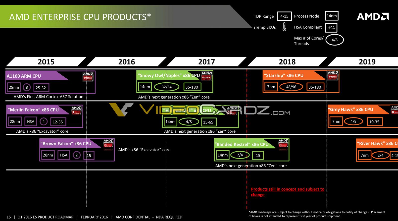
A 48 core would be 12 ccx (6 zeppelin equivalent). [See image below for logic. 48Core Starship and perhaps more relevantly, 4core Grey Hawk]
NTMBK
Lifer
- Nov 14, 2011
- 10,526
- 6,051
- 136
But how do you make a die of 3 ccx? would have to be a very "long" die but nor sure that is a problem but maybe could be due to package size.
Hmm, good point. Maybe they could change the internal layout of a CCX, so that instead of a 2x2 tile it's a 1x4? *not a processor engineer*
I think the new AMD is going to make as few fundamental changes as possible for the needed performance. We are seeing their philosophy as getting the most out of as little as possible starting to payback in a big way. Don't expect that to change for the next few years at least.Hmm, good point. Maybe they could change the internal layout of a CCX, so that instead of a 2x2 tile it's a 1x4? *not a processor engineer*
mattiasnyc
Senior member
- Mar 30, 2017
- 356
- 337
- 136
Not sure that a 6 core CCX makes that much sense- you're boosting the intra-CCX latency. My personal guess would be that they go to 3x4 per die, rather than 2x6.
Do you mean latency within one CCX? Isn't the bigger issue the latency between CCX? If so it would seem that more cores per complex increases the chances of not needing to go outside to get data, and conversely that more CCX = more large-latency hits.
LightningZ71
Platinum Member
- Mar 10, 2017
- 2,717
- 3,423
- 136
I'm not sure that a 6 core ccx makes much sense from a layout point of view. I would imagine that it has other internal addresting issues to contend with. Instead, I would imagine that with their current packaging dimensions, you could see a switch to 4 CCXS per chip. Or, as an alternative, continue with two CCXs, but add an "L4 cache" that is on the order of 256MB or larger.
Assuming that they stay with similar dimensions to the current dies, and that the physical interface sections of the dies can't shrink much more to maintain the ability to link to the substrate traces, the CCXS will have to change layout to fit if they are larger than 6 cores and keep a double row arrangement. If they rotate the ccx units 90 degrees, then they can fit two rows of 4 with a common L3 between the rows. That's going to allow the L3 to double, but will likely add a bit of latency for DRAM controller access due to a longer routing trace in the chip. All of that is contingent on there being no major changes to the relative core dimensions with the shrink and revision.
Again, I'm no expert and this is just my opinion.
Last edited:
Not sure that a 6 core CCX makes that much sense- you're boosting the intra-CCX latency. My personal guess would be that they go to 3x4 per die, rather than 2x6.
How much would the latency increase, especially on GF's 7FF? I don't know either, but I'm sure it would be worth it rather than having more inter-CCX latency. It's a matter of design and AMD has known for a while what they want @ 7nm. We will see if AMD had the $$s to redesign the CCX after two iterations. If they did redesign it, they can go with an APU with up to six cores using just one CCX.
Edit: didn't see that roadmap posted by Atari2600. So the answer is that AMD is sticking with a 4 core CCX. It certainly makes sense financially.
Edit2: Dang slide is from a clickbait site

Last edited:
T1beriu
Member
- Mar 3, 2017
- 165
- 150
- 81
Edit2: Dang slide is from a clickbait site
I would freak out as well, but the original source for the slide is the opposite of a clickbait site.
They have. Already announced and up on their webpage.If they build supermicro 1s boards I might consider buying EPYC. Seems Intel is leaving out 1s support with the Purley platform.... Not really happy about that...
https://www.supermicro.com/products/nfo/AMD_SP3.cfm?pg=MOBO
You will find them here. Supermicro Epyc Servers and MotherboardsIf they build supermicro 1s boards I might consider buying EPYC. Seems Intel is leaving out 1s support with the Purley platform.... Not really happy about that...
Markfw
Moderator Emeritus, Elite Member
- May 16, 2002
- 27,414
- 16,274
- 136
Wow. I just figured this out.... The most I can find for DDR4 ECC registered is 64 gig modules. That motherboard I saw (H11DSi) has 16 slots and supports up to 2 TB memory 2666. So for 1 TB (64*16) DDR4 2133 (fastest I could find) and 2 32 core, 64 thread CPU's, and just guessing on $1000 motherboard with HSF's that 25k for 128 threads, and 1 TB memory, just WOW, not bad (for enterprise class hardware)
The memory was $1849 for 2 64 gig memory sticks = ~15k + mobo+ 8k for 2 processors.
The memory was $1849 for 2 64 gig memory sticks = ~15k + mobo+ 8k for 2 processors.
thecoolnessrune
Diamond Member
- Jun 8, 2005
- 9,673
- 583
- 126
Wow. I just figured this out.... The most I can find for DDR4 ECC registered is 64 gig modules. That motherboard I saw (H11DSi) has 16 slots and supports up to 2 TB memory 2666. So for 1 TB (64*16) DDR4 2133 (fastest I could find) and 2 32 core, 64 thread CPU's, and just guessing on $1000 motherboard with HSF's that 25k for 128 threads, and 1 TB memory, just WOW, not bad (for enterprise class hardware)
The memory was $1849 for 2 64 gig memory sticks = ~15k + mobo+ 8k for 2 processors.
I know through my workplace that HP has validated DDR4 2400 128GB 8x rank DIMMs. You'll pay a premium for them though.
https://www.cdw.com/shop/products/HPE-DDR4-128-GB-LRDIMM-288-pin/4286681.aspx#POTRENDING THREADS
-
 Discussion Zen 5 Speculation (EPYC Turin and Strix Point/Granite Ridge - Ryzen 9000)
- Started by DisEnchantment
- Replies: 25K
-
Discussion Intel Meteor, Arrow, Lunar & Panther Lakes + WCL Discussion Threads
- Started by Tigerick
- Replies: 24K
-
 Discussion Intel current and future Lakes & Rapids thread
- Started by TheF34RChannel
- Replies: 23K
-

-

AnandTech is part of Future plc, an international media group and leading digital publisher. Visit our corporate site.
© Future Publishing Limited Quay House, The Ambury, Bath BA1 1UA. All rights reserved. England and Wales company registration number 2008885.