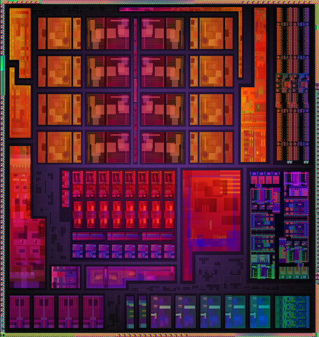
Fresh leak out today, not much is known but at least 8cu's is confirmed. Probably an engineering sample, core count is unknown and clocks may not be final.
This is very interesting to me because cezanne is seemingly 8cu only, and it seems unlikely to me that AMD could squeeze any more performance out of vega. A cpu only upgrade of renoir may be lackluster compared to tigerlake's quite large GPU.
What do you guys think? Will zen 3 be a large enough improvement in APU form? Will it have full cache? Are there more than 8cus? Has AMD truly evolved vega yet again or is it more like rdna?
")