If AMD goes for core-count advantage with Zen 2 against Skylake/CFL, I see that as a poor sign for competitive single-thread performance. Personally, I still expect 7nm Zen 2 to beat 14nm Skylake/CFL. Anything less would be poor planning against 10nm Ice Lake, which would have been here by now, had Intel not stumbled so badly.
I'm going to try and take a different angle to this.
What I see is a company that is planning a roll-out strategy of a number of different technologies over the course of a number of different advances in production capability. On the production side we've got a 2:1 shrink, a follow-on that reduces power-use but doesn't do much for size, and another shrink, but one that isn't at all as large as the move from 14 to 7nm. On the technology side we've got moar-cores, power budgets, signal routing/connectivity, frequency -- feel free to add your own.
A company that doesn't go for core count on the 2:1 shrink isn't targeting well. That means they've got to think about how to deliver the core count without blowing the budget (chiplets), how to connect all the cores, how to feed the cores (tech they haven't yet disclosed), etc. These are the engineering challenges that are front of mind. Now add marketing. Marketing comes in and says, ok, how to best sell more cores -- what market are we hitting? You ask about single-thread performance. Where are frequency concerns in servers? Well, we've already heard them say that they have customers that want high frequency, low-core count parts. That isn't the gaming market, sure, but it's a concern that at least isn't lost in this round. You heard the AMD server guy who said "hey, this part isn't a desktop part that's pretending to be a server chip" (or words to that effect). While it wasn't clear to me whether he was talking about Intel or AMD parts, the point is that THIS is the server chip. It isn't targeting the desktop. It remains to be seen whether the desktop part is a repurposed server chip, or a purpose-built desktop chip, but given Intel's missteps, if AMD has gotten decent IPC and frequency uplifts, they could get away with it. Big time.
I think it would be hard to be disappointed that AMD is targeting the server market with higher core counts while still recognizing the importance of more performant, lower core-count parts. They're leading with the strengths of the node, adding the floating point vectors that they need to compete, but not going overboard with a full 512 implementation. Power-reduction cycle would be next, so I half expect for laptops to be targeted for 7nm+. I don't know whether you create a fused 7nm design on this go-around, but it seems smart for the low-power market, so I'd certainly expect such a development on 7nm+, regardless of whether it happens this time. Maybe you add the half-width 512 ops in that round, and in the 5nm shrink you go wider on the floating point units. Or maybe you redesign your GPU to better integrate with your CPUs, and provide something that's more flexible. Worrying about this in a couple of years allows Lisa to steer the Radeon ship safely back into port.
So far, honestly, I'm pretty impressed. I don't know if they'll deliver the parts *I* want, but they're targeting the market that the node move will have the biggest impact on, and they're focusing their engineering effort there, rather than being distracted by the rest of the market.
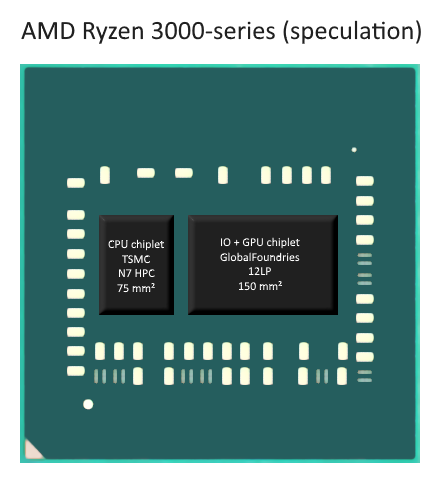
Yeah. I wouldn't be surprised if we see Threadripper 3000 before Ryzen 3000. All the components are there for Threadripper, since it is all reuse of the EPYC platform. Ryzen 3000 either needs an IO chiplet or a monolithic design. I bet on the former.
Ditto. I also wouldn't be surprised if there was a little something extra on TR3. They might wait until TR4, but, I don't think you try to feed a 64 core TR4 through 4 memory channels. Max it out at 48, and sprinkle a little pixie dust in-between. GPU cores? FPGA chiplets? What sort of crazy hackathon projects have the engineers prepared this go-around? Could get interesting....