Why Intel 14nm was named ...14nm?

t1gran

Member
Jun 15, 2014
34
1
71
1) Could someone make clear this question please? I know that different chip-makers differently name their manufacturing process, and it is rather a marketing term. Wikipedia says that the naming of this technology node as "14 nm" came from the International Technology Roadmap for Semiconductors (ITRS). So does it mean "14 nm" is an abstract term, which dose not refer to any transistor's component? Then why 14 nm and not 16 nm?

2) As far as I know quantum effects will arise when transistor gate pitch becomes less than 5-1 nm. According to Intel transistor gate pitch in it's 14 nm Process Technology is 70 nm. Does it mean that 5-1 nm is far, far away, and it's not correct to make forecasts based on today's marketing "14 nm"?

3) Won't it be more correct to compare actual number of transistors per square mm - instead of all these nanometers? Or transistors on different chips are also of different size?
 

witeken

Diamond Member
Dec 25, 2013
3,899
193
106
Excellent question.

(2) To answer your second question first: gate length !!!!!= gate pitch (from your 5-1nm range I suspecr you've read the 1nm gate length transistor article). Gate pitch is distance between gates of two transistors. Gate length of Intel's 14nm is 20nm. Of course, the limiting factor will be the gate length because the gate pitch will always be bigger than the gate pitch. So it's already pretty small, but there's still a lot of froom left.

(1) Intel named 14nm 14nm instead of 16nm (which is 22 / sqrt(2)) because Intel decided to shrink by a larger amount than they had historically done every node. They decided to do that at 14nm because at 14nm wafer cost began to rise more than it had historically done. In that way, they would ensure that the price per transistor would reduce the same as it had done historically.

Chart-4.png


The price per transistor was a real concern because for instance Nvidia complained that it would stay flat for TSMC.

IBS-1.jpg


To be honest, the veracity of this is not known and probably a bit exaggerated, but the trend is clear in any case.

Now, this 14nm number only represents Intel's feeling that they would shrink more than usually, but it does not refer, just like any other node name by any other company, to an actual transistor feature size.

So the reason it's 14nm is completely historical: Moore's Law said transistor size had to shrink by 0.7 every generation to get 0.7²=0.5 area reduction for double the x'tor density. However, not every feature was shrunk by that much. In the midst of the GHz race, the gate length was shrunk more than the area to gain higher clock speeds. However, the node name did not reflect this. So every generation the name was reduced by 0.7x, but the area was almost never 0.5x. So the name shrunk more than the transistor.

And that's why people now think that transistors are now very near the atomical level and so Moore's Law will end soon. But that's also exaggerated.

(3) No, transistors per mm² also isn't the best way to compare nodes. This is because transistors in reality aren't packed together as close as they can: they are connected by interconnects and they are designed by architects to form logic circuits that can do processing. So transistor density is impacted by those design decisions. For instance, a chip full of NAND (called an SSD) has easily >10x more transistors than a processor.

However, a meaningful way to compare nodes is to look at SRAM (which is a form of fast memory that is used in processors) size because those are a standard feature made up of 6 transistors.

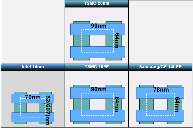
TSMC 16nm = 0.07µm² (high density)
Samsung 14nm = 0.080µm² / 0.064µm² (high density)
Intel 14nm = 0.0588µm² / 0.0500µm²
 
Last edited:
Mar 10, 2006
11,715
2,012
126
Intel originally called this node 16nm, then renamed it to 15nm, then renamed it again to 14nm. :p
 

t1gran

Member
Jun 15, 2014
34
1
71
Witeken
Thanks a lot a for your explanations, I learned a lot from you.
from your 5-1nm range I suspecr you've read the 1nm gate length transistor article
Exactly, I'm not good in English and thought they were synonyms.

A few more questions if you don't mind:
1) Is there any reliable source for "gate length of Intel's 14nm is 20nm"?

2)
They decided to do that at 14nm because at 14nm wafer cost began to rise more than it had historically done
Did you mean "because at 16nm wafer cost began to rise more than it had historically done"? Otherwise I don't understand.

3) Do you agree with this? The author says Intel's nanometer = 1.182 x real nanometer (1.182 = 26 / 22, 16.55 / 14), and also says "Which puts Intel’s 14nm process pretty much on a par with the foundry industry’s 20 nanometre process, and behind TSMC’s 16 nanometre finfet process and Globalfoundries’ 14nm process". Actually there is technical difference between 16nm and 14nm, isn't there?

4) What about TSMC 16nm and Globalfoundries 14nm - do they reflect their real gate's length?

5)
No, transistors per mm² also isn't the best way to compare nodes. This is because transistors in reality aren't packed together as close as they can: they are connected by interconnects and they are designed by architects to form logic circuits that can do processing. So transistor density is impacted by those design decisions. For instance, a chip full of NAND (called an SSD) has easily >10x more transistors than a processor.
I thought that considering processors only (not DDR, NAND etc), transistor density better reflects Moore's attitude to progress. So processor with less transistors can outperform one with more transistors, can't it?

5)
However, a meaningful way to compare nodes is to look at SRAM (which is a form of fast memory that is used in processors) size because those are a standard feature made up of 6 transistors.

TSMC 16nm = 0.07µm² (high density)
Samsung 14nm = 0.080µm² / 0.064µm² (high density)
Intel 14nm = 0.0588µm² / 0.0500µm²
The lesser - the better? May I also ask you for source of this information (just to cite it in similar discussions)?
 

witeken

Diamond Member
Dec 25, 2013
3,899
193
106
Witeken
Thanks a lot a for your explanations, I learned a lot from you.
You're welcome :).

A few more questions if you don't mind:
1) Is there any reliable source for "gate length of Intel's 14nm is 20nm"?
Yes, Intel's 2014 presentation at the International Electron Devices Meeting (IEDM): http://www.intel.com/content/dam/ww...foundry/intel-14nm-iedm-2014-presentation.pdf.

2)
Did you mean "because at 16nm wafer cost began to rise more than it had historically done"? Otherwise I don't understand.
No, at Intel's 14nm node. It doesn't matter how you call it. At that node, they (and other companies too like Samsung and TSMC) had to start using something called double patterning, which means that you have to expose the wafer twice to do one step. So wafer costs rose something like 30%. To counteract this rising wafer cost, they tried to make the transistor smaller than usual, to get as much benefit from the two exposures as possible.

3) Do you agree with this? The author says Intel's nanometer = 1.182 x real nanometer (1.182 = 26 / 22, 16.55 / 14), and also says "Which puts Intel’s 14nm process pretty much on a par with the foundry industry’s 20 nanometre process, and behind TSMC’s 16 nanometre finfet process and Globalfoundries’ 14nm process". Actually there is technical difference between 16nm and 14nm, isn't there?
No, this is a completely incorrect article from someone who has incomplete knowledge. As you have seen, so far I have only given you information about Intel's gate length. So if you only knew Intel's gate length, which was indeed 26nm at their 22nm node, then you see that it's pretty close to that 22nm number, but in fact a bit bigger. So I suppose that he thought that node number = gate length, which has never been the case. However, if I now cherry pick another number, you would think exactly the opposite: Intel's 90nm node had a gate length of 45nm. Here are some other values:

http://www.extremetech.com/wp-content/uploads/2013/07/transistor-gate-length-scaling.jpg

You really have to step away from the node number if you want to get some knowledge of the actual transistor. The node number does litterally not mean anything. For instance, TSMC's 16nm is exactly as big as its 20nm in terms of x'tor density.

4) What about TSMC 16nm and Globalfoundries 14nm - do they reflect their real gate's length?
I don't know their gate length, I'm not sure if they have disclosed that number. However, some companies measure it themselves. According to TechInsights, Samsung is ~30 and TSMC is ~33. But given they report ~24 for Intel, I don't know how reliable that information is. http://www.electronics-eetimes.com/news/samsung’s-14-nm-lpe-finfet-transistors/page/0/3

I do want to add however that gate length typically is not really all the important for density. For density, which is what people always assume the nm number to refer to, you have to look at gate pitch and interconnect pitch. They give you a proxy for area.

Cell-SizeComparison.png


5)
I thought that considering processors only (not DDR, NAND etc), transistor density better reflects Moore's attitude to progress. So processor with less transistors can outperform one with more transistors, can't it?
It depends of course. But realize that nowadays processors contain much more than just the execution units. Intel's processors also come with integrated graphics, etc.

5)
The lesser - the better? May I also ask you for source of this information (just to cite it in similar discussions)?
Source for what?
 
  • Like
Reactions: MongGrel and t1gran

witeken

Diamond Member
Dec 25, 2013
3,899
193
106
@Arachnotronic

I meant these figures you gave relating SRAM:
TSMC 16nm = 0.07µm² (high density)
Samsung 14nm = 0.080µm² / 0.064µm² (high density)
Intel 14nm = 0.0588µm² / 0.0500µm²

Samsung (the 0.04 and 0.049 are Samsung 10nm): http://www.eetimes.com/document.asp?doc_id=1328866 (x*0.62=0.040 <=> x = 0.064)

Samsung-10nm-performance-x-800.png


Or alternatively: http://electroiq.com/wp-content/uploads/2014/02/6.png

6.png


Intel, TSMC, Samsung:

29ae1e9b55341810f46ba5d13912927feee2d2a3


Intel high density: https://twitter.com/thekanter/status/552722977058721792

Or alternatively: http://pc.watch.impress.co.jp/docs/news/event/707682.html

photo005.jpg


Via http://www.realworldtech.com/forum/?threadid=151396&curpostid=151470

AFAIK Intel doesn't use the 0.05µm² ones, but foundry customers could.

So just notice how close Samsung's 10nm SRAM is to Intel's 14nm. Only 20% smaller.
 
Last edited:
  • Like
Reactions: T1beriu and t1gran
Mar 10, 2006
11,715
2,012
126
  • Like
Reactions: Dresdenboy
Mar 10, 2006
11,715
2,012
126

There are question marks on the 16nm fin height lol

Anyway witeken, you will be pleased to know that Intel's 14nm is likely substantially ahead of TSMC and Samsung processes in terms of transistor drive strength, and 14nm+ likely even further ahead. Fin height is a key characteristic that impacts finfet drive strength and it looks like Intel has the foundries beat here.
 
  • Like
Reactions: witeken

witeken

Diamond Member
Dec 25, 2013
3,899
193
106
There are question marks on the 16nm fin height lol

Anyway witeken, you will be pleased to know that Intel's 14nm is likely substantially ahead of TSMC and Samsung processes in terms of transistor drive strength, and 14nm+ likely even further ahead. Fin height is a key characteristic that impacts finfet drive strength and it looks like Intel has the foundries beat here.
Wait, did you mean to convey information in your post that I did not yet know :D?
 

witeken

Diamond Member
Dec 25, 2013
3,899
193
106
There are question marks on the 16nm fin height lol

Anyway witeken, you will be pleased to know that Intel's 14nm is likely substantially ahead of TSMC and Samsung processes in terms of transistor drive strength, and 14nm+ likely even further ahead. Fin height is a key characteristic that impacts finfet drive strength and it looks like Intel has the foundries beat here.
Although I wonder how much of an impact it actually has. Intel increased fin height from 32nm to 42nm and TSMC/Samsung are in between those 2 values. And it isn't like 14nm overclocks dramatically better than 22nm.
 
Mar 10, 2006
11,715
2,012
126
Although I wonder how much of an impact it actually has. Intel increased fin height from 32nm to 42nm and TSMC/Samsung are in between those 2 values. And it isn't like 14nm overclocks dramatically better than 22nm.

Intel 22nm was 34nm I believe, so it looks like the foundries came closer to Intel 22nm than they did to 14nm...I didn't expect this from just plain eyeballing the fin heights, but there it is.
 
  • Like
Reactions: witeken

witeken

Diamond Member
Dec 25, 2013
3,899
193
106
Intel 22nm was 34nm I believe, so it looks like the foundries came closer to Intel 22nm than they did to 14nm...I didn't expect this from just plain eyeballing the fin heights, but there it is.
Intel's no fool ;).

“It's a true [Intel] 14nm technology. There's lots of 14nm technologies around, and they're not all created equal.” --William Holt, Intel, IM’14

“That still is 3 and a half years that we have built and experience and also shipping. I'm not going to tell you what the next innovations are, but our roadmap is full, because to continue to improve transistors, you have to make substantial improvements. And we plan to do that, while other people are working on perfecting their FinFET devices, and we're gonna be moving on to looking at what comes next.” --William Holt, Intel, IM’14

But wait, aren't you that same guy who said a few hours ago that I shouldn't be so bothered with the technical details because they don't give Intel foundry wins :)?
 
Mar 10, 2006
11,715
2,012
126
But wait, aren't you that same guy who said a few hours ago that I shouldn't be so bothered with the technical details because they don't give Intel foundry wins :)?

You can't win fab deals on technology alone. I just find this stuff interesting for its own sake :)
 
  • Like
Reactions: witeken

witeken

Diamond Member
Dec 25, 2013
3,899
193
106
You can't win fab deals on technology alone. I just find this stuff interesting for its own sake :)
Yeah, Intel has the tallest fins, the densest fins, the most rectangular fins, the shortest gate length (I didn't know at all that Samsung and TSMC were still in the 30s LOL even worse than 22nm o_O), the best air gapped interconnect, the smallest interconnect, the least variation, the highest drive current, the steepest sub threshold slope and threshold voltage, the highest yield and the earliest time to market. I don't care what you call this, but this technology is very decent.
 
Last edited:

wingman04

Senior member
May 12, 2016
393
12
51
Yeah, Intel has the tallest fins, the densest fins, the most rectangular fins, the shortest gate length (I didn't know at all that Samsung and TSMC were still in the 30s LOL even worse than 22nm o_O), the best air gapped interconnect, the smallest interconnect, the least variation, the highest drive current, the steepest sub threshold slope and threshold voltage, the highest yield and the earliest time to market. I don't care what you call this, but this technology is very decent.
From what you said what can Intel improve upon past the kaby lake 14nm+.
 

superstition

Platinum Member
Feb 2, 2008
2,219
221
101
Yeah, Intel has the tallest fins, the densest fins, the most rectangular fins, the shortest gate length (I didn't know at all that Samsung and TSMC were still in the 30s LOL even worse than 22nm o_O), the best air gapped interconnect, the smallest interconnect, the least variation, the highest drive current, the steepest sub threshold slope and threshold voltage, the highest yield and the earliest time to market.
And dubious TIM for its enthusiast quad line.
 

ehume

Golden Member
Nov 6, 2009
1,511
73
91
Perhaps they can make their fins eve3n taller and go back to soldering their CPU's.
 

witeken

Diamond Member
Dec 25, 2013
3,899
193
106
From what you said what can Intel improve upon past the kaby lake 14nm+.
Well, at 10nm the most important thing they could do are:

  • Put fins (and interconnect wires and gates) even closer together (for about 2x more transistors/mm²)
  • Make gate even shorter
  • Put III-V and Ge in the channel for higher performance (mobility) and (potentially vastly improved?) lower power
  • Improve the fin with a quantum well, which will result in 3 sides being controlled by gate + the 4th side isolated
We'll just have to see what they have done. It's been a long time since 14nm+10nm density plans were disclosed (3 years now) and 2 years since 14nm transistor briefing, and it will still be another year until the new transistor gets released :(.