Discussion RDNA4 + CDNA3 Architectures Thread

Page 93 - Seeking answers? Join the AnandTech community: where nearly half-a-million members share solutions and discuss the latest tech.

DisEnchantment

Golden Member
Mar 3, 2017
1,747
6,598
136
1655034287489.png
1655034259690.png

1655034485504.png

With the GFX940 patches in full swing since first week of March, it is looking like MI300 is not far in the distant future!
Usually AMD takes around 3Qs to get the support in LLVM and amdgpu. Lately, since RDNA2 the window they push to add support for new devices is much reduced to prevent leaks.
But looking at the flurry of code in LLVM, it is a lot of commits. Maybe because US Govt is starting to prepare the SW environment for El Capitan (Maybe to avoid slow bring up situation like Frontier for example)

See here for the GFX940 specific commits
Or Phoronix

There is a lot more if you know whom to follow in LLVM review chains (before getting merged to github), but I am not going to link AMD employees.

I am starting to think MI300 will launch around the same time like Hopper probably only a couple of months later!
Although I believe Hopper had problems not having a host CPU capable of doing PCIe 5 in the very near future therefore it might have gotten pushed back a bit until SPR and Genoa arrives later in 2022.
If PVC slips again I believe MI300 could launch before it :grimacing:

This is nuts, MI100/200/300 cadence is impressive.

1655034362046.png

Previous thread on CDNA2 and RDNA3 here

 
Last edited:

Mahboi

Golden Member
Apr 4, 2024
1,035
1,899
96
Wait hold on here, his video is a goldmine of an IQ test.
1714245018863.png
600% increase in RT to be on par with Blackwell.
You heard it at RGT's first!
1714245060393.png
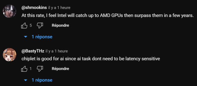
"Intel is just better as Alchemist has proven"
"AI doesn't care about latency so just kill the latency with your latency heavy chiplets"
1714245279574.png
Someone who as a real 6900xt that really exists and as no reason to buy anything but Nvidia but as a 6900 xt because here is no reason to buy high end AMD.
He could stand to ave a english lesson too.

Before someone says "it's lowbrow to pick and mock them", hey they started picking things here first, it's only fair. And funny.
 

gaav87

Member
Apr 27, 2024
168
350
96
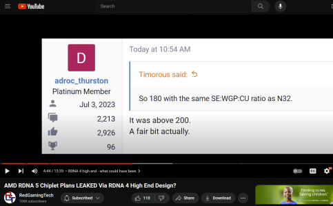
Shader engines. N44 has 2 N48 has 4. The code shown has SEs 0 through 8 for 9 SEs which would be a 144CU (or 180 if they had the same layout as N32) design and would fit with the 3 GCDs of 3SEs each that was rumoured for N4C ages ago.

Thats interesting.
But you can't be sure N48 has 4 as recent leaks pointed it having 50TFLOPs of FP32.
9(vector units) x 32(wide) x 64cu x clock speed /1,000,000 = 50
Means, a boost clock speed of ~2713mhz

vs (rdna 3 design with dual issue)
4 (vu) x 2 x 32(wide) x 64cu x clock speed /1,000,000=50
~3050mhz boost clock

I would lean on ~2700mhz reference boost clock (200-300mhz higher then rdna3) vs 3050mhz (crazy clock speed)
Also this would mean they ditched dual issue fp32 and went with similar design to intel bmg with more thread count for literally 2x 6950xt compute performance.
But idk how did they manage to fit that on ~255mm2 so maybe i am talking bs.

All_The_Watts leaked:
N48
+50TFLOPs fp32
32
64
256
693
2770
~240 mm²
 
Last edited:

Timorous

Golden Member
Oct 27, 2008
1,770
3,322
136
Thats interesting.
But you can't be sure N48 has 4 as recent leaks pointed it having 50TFLOPs of FP32.
9(vector units) x 32(wide) x 64cu x clock speed /1,000,000 = 50
Means, a boost clock speed of ~2713mhz

vs (rdna 3 design with dual issue)
4 (vu) x 2 x 32(wide) x 64cu x clock speed /1,000,000=50
~3050mhz boost clock

I would lean on ~2700mhz reference boost clock (200-300mhz higher then rdna3) vs 3050mhz (crazy clock speed)
Also this would mean they ditched dual issue fp32 and went with similar design to intel bmg with more thread count for literally 2x 6950xt compute performance.
But idk how did they manage to fit that on ~255mm2 so maybe i am talking bs.

All_The_Watts leaked:
N48
+50TFLOPs fp32
32
64
256
693
2770
~240 mm²

2770 is effective bandwidth if you account for infinity cache. Or was, if the memspec is 18gbps then the bandwidth and effective bandwidth both drop from those rumours.
 

branch_suggestion

Senior member
Aug 4, 2023
408
901
96
Thats interesting.
But you can't be sure N48 has 4 as recent leaks pointed it having 50TFLOPs of FP32.
9(vector units) x 32(wide) x 64cu x clock speed /1,000,000 = 50
Means, a boost clock speed of ~2713mhz

vs (rdna 3 design with dual issue)
4 (vu) x 2 x 32(wide) x 64cu x clock speed /1,000,000=50
~3050mhz boost clock

I would lean on ~2700mhz reference boost clock (200-300mhz higher then rdna3) vs 3050mhz (crazy clock speed)
Also this would mean they ditched dual issue fp32 and went with similar design to intel bmg with more thread count for literally 2x 6950xt compute performance.
But idk how did they manage to fit that on ~255mm2 so maybe i am talking bs.

All_The_Watts leaked:
N48
+50TFLOPs fp32
32
64
256
693
2770
~240 mm²
But it is ((128ALU*64CU*3050Mhz)*2)/1000000 = ~50TF
RDNA3 missed clock targets at TBP significantly. 64CU only makes sense for 2 or 4SE, you will see the 2SE version more or less with the PS5 Pro.
Not much longer now until we see the true clock speeds realised.
 

gaav87

Member
Apr 27, 2024
168
350
96
But it is ((128ALU*64CU*3050Mhz)*2)/1000000 = ~50TF
RDNA3 missed clock targets at TBP significantly. 64CU only makes sense for 2 or 4SE, you will see the 2SE version more or less with the PS5 Pro.
Not much longer now until we see the true clock speeds realised.
Im talking most basic fundamental level. Amd executes workloads in groups of 32 threads(32wide) each capable of same result calculation on port0 + port1 (dual issue).
16 wave per SIMD(VALU)
4 SIMD per WGP

1 (INT32 Ops per Clock (ADD) x16 (wave) x 4(simd) x 64cu x 3050mhz )x2 (dual issue) =25 TFLOPs INT32
2 (FP32 FLOPs per Clock (MAD) x16 (wave) x 4(simd) x [32WGP (2 wgp per cu)=64CU] x 3050mhz )x2 (dual issue) =50 TFLOPs FP32
=4096(VALU)
Each 1 VALU can do 2 fp32 FLOPs per clock or 1 int32 ops per clock.

They either
- increased wave count from 16 to 32
- Made the simd 64 wide instead of 32 (simmilar to GCN)
- increased WGP per shader engine from 8 to 9
- Got rid of dual issue on port0 and port1
All this points to ~2700-2750mhz boost

Or left it as in rdna3 and the clock is 3050mhz but its highly unlikely too high boost clock.

Or the 50TFLOPs leak is just bs :)
 

Attachments

  • amdrdna3.jpg
    amdrdna3.jpg
    108.2 KB · Views: 20
Last edited:

Mahboi

Golden Member
Apr 4, 2024
1,035
1,899
96
Navi WGPs Bus GDDR Generation

Wut?
The second column has to be workgroups.
RDNA 4 aimed at 144 WGPs and 5 for more than that? And more than 384 bit bus?
 

gaav87

Member
Apr 27, 2024
168
350
96
Which is not unrealistic, it is a new uArch and has a nodelet bump.
Throw in RDNA3 being a low barrier to beat due to clocks eating power and it is possible.
Scale off Ada and it also checks out.
We do not know that. But i think its more likely then 3050mhz clock that amd increased per-SIMD matrix multiplication. Maybe they changed simd width or increased simd count per wgp leaving wave slots at 16 or lowered wave slots even more they went from 20 to 16 rdna2->rdna3 but each simd can operate 32 slots this would make sense that they introduced SWMMAC. Lowering wave slots would lower occupancy lowering latency and increasing performance.
 

TESKATLIPOKA

Platinum Member
May 1, 2020
2,554
3,100
136
I find It unrealistic that N41 with 3x more WGPs was planned with the same bus width as N48.
Yes, It uses GDDR7, but that will provide ~50-60% more BW compared to GDDR6.
 
  • Like
Reactions: Tlh97

Tigerick

Senior member
Apr 1, 2022
701
628
106

Quite sad to see the N40 and N41 canned. Looks like an ambitious design to say the least.
Let's try to combine RDNA4 and RDNA5 in the table below:

CodenameBase DieWGPCUGDDR6Memory SpeedMemory BW
RDNA4
N441163216GB 128-BIT18 Gbps288 GB/s
N481326416GB 256-BIT18 Gbps576 GB/s
RDNA5GDDR7
N5229619216GB 256-BIT32 Gbps1024 GB/s
N51314428824GB 384-BIT32 Gbps1536 GB/s
N50419238432GB 512-BIT32 Gbps2048 GB/s

  • I assumed upcoming N51 and N52 are replacing N41 and N42 with updated design and architecture. I also assume N52 is using two base dies with 128-BIT GDDR7 memory bus each. Will update if any new info appears...
  • There are power and bandwidth penalty with chiplet design. That's mean game clock might not able to clock as high as monolithics design. That's why I expect AMD will use 32Gbps GDDR7.
  • That might explain why AMD is putting 3 times CU with 78% extra memory bandwidth. Also remember AMD might be binning the die for N52.
  • Remember upcoming RTX5090 comes with 512-bit memory bus as well, and that's the target of N50. RTX5090 comes with 192 SM which is similar to N50's 192 WGP. Of course, NV and AMD might not be using full die but the similarities amount of SM and WGP is interesting.
 
Last edited:

Tigerick

Senior member
Apr 1, 2022
701
628
106
Not similar
RX 7600 16WGP - RTX 4060 24SM
RX 7800XT 30WGP - RTX 4070 46SM/4070Super 56SM
RX 7900XT 42WGP - RTX 4070ti 60SM/RTX 4070ti Super 66SM
RX 7900XTX 48WGP - RTX 4080 76SM/RTX 4080super 80SM
Ho, you should check GB202's SM amount. And if my speculation is correct, upcoming GB203 should come with 144SM and GB205 should come with 80SM. Go figure...
 

branch_suggestion

Senior member
Aug 4, 2023
408
901
96

Quite sad to see the N40 and N41 canned. Looks like an ambitious design to say the least.
16WGP per SED, I wonder the SA config.
We do not know that.
It is the first GPU in a long time that has >20% perf headroom with pushing power beyond the design power. The thing is broken.
But i think its more likely then 3050mhz clock that amd increased per-SIMD matrix multiplication. Maybe they changed simd width or increased simd count per wgp leaving wave slots at 16 or lowered wave slots even more they went from 20 to 16 rdna2->rdna3 but each simd can operate 32 slots this would make sense that they introduced SWMMAC. Lowering wave slots would lower occupancy lowering latency and increasing performance.
Well RDNA4 does aim to simplify the WGP in clever ways to make it more spammable. That would only make clocks go even higher, rather than increasing per unit throughput.
Ho, you should check GB202's SM amount. And if my speculation is correct, upcoming GB203 should come with 144SM and GB205 should come with 80SM. Go figure...
Not a chance in a million years that a BW SM will be equivalent to an RDNA4/5 WGP.
Stop pretending that you know anything, I grow tired of it

.
 

Tigerick

Senior member
Apr 1, 2022
701
628
106
16WGP per SED, I wonder the SA config.

It is the first GPU in a long time that has >20% perf headroom with pushing power beyond the design power. The thing is broken.

Well RDNA4 does aim to simplify the WGP in clever ways to make it more spammable. That would only make clocks go even higher, rather than increasing per unit throughput.

Not a chance in a million years that a BW SM will be equivalent to an RDNA4/5 WGP.
Stop pretending that you know anything, I grow tired of it

.
Then ignore me, thank you