- Mar 3, 2017
- 1,608
- 5,816
- 136

I disagreeI don't think STX lineup is monolithic.
")
You're comparing apples and oranges. The density of a high speed, cache-heavy compute die will be vastly different from an SoC with a GPU and everything else included. I'm sure if you actually look at the Zen 4 cluster in isolation, the density will be very similar to the desktop Zen 4.
What are the specific issues you see, do you guys have lots of manual stuffs in your physical design flows, timings, physical layout, floor plan, routing etc.I wouldn't lean so heavily on TSMC's talk of FinFlex. The reality is that while it makes for some convenient libraries at times, it's a real PIA to use, perhaps more than it's worth in many cases. Would hate to make a full SoC out of it.
Curious question: How many chips on average are killed during development while silicon engineers are testing their voltage/current max limits?What are the specific issues you see, do you guys have lots of manual stuffs in your physical design flows, timings, physical layout, floor plan, routing etc.
At least for us once specific cells for the PDK has been customized (which I doubt if at all we are doing something with it) our favorite tool can do much of the rest automatically for each macro.
I have no idea, I am managerial staff now but for us I bet more chips gets killed by temperature tests because our target applications has much wider operating ranges. Voltage/Current is not a big issue for applications wherein the user cannot tinker with the system.Curious question: How many chips on average are killed during development while silicon engineers are testing their voltage/current max limits?
I would think that a chip with 25bn xtors is way, way too much to do by hand. I think it's been that way quite a while, especially at AMD. Aside from floor-plan layouts (need IO ports on this side, need DRAM interface on this side, etc) - I would doubt anything is hand tuned. Just block level logic and cache optimized for high performance and then the Cadence/Synopsis servers go Brrrrrrr.What are the specific issues you see, do you guys have lots of manual stuffs in your physical design flows, timings, physical layout, floor plan, routing etc.
At least for us once specific cells for the PDK has been customized (which I doubt if at all we are doing something with it) our favorite tool can do much of the rest automatically for each macro.
However, we are on a much older node.
According to rumors apparently some company is tinkering with their macros/IP blocks by hand heavilyI would think that a chip with 25bn xtors is way, way too much to do by hand. I think it's been that way quite a while, especially at AMD. Aside from floor-plan layouts (need IO ports on this side, need DRAM interface on this side, etc) - I would doubt anything is hand tuned. Just block level logic and cache optimized for high performance and then the Cadence/Synopsis servers go Brrrrrrr.
Can you hazard a guess which company that might be? I don't think there can be many in this space. Seems like a really specialized field, similar to ASML's.According to rumors apparently some company is tinkering with their macros/IP blocks by hand heavily
Sounds a lot like chipset disaggregation with north- and southbridge.So my thought was that the only die-to-die connections are from the IOD-fast to each other die, so that would take care of the big-ticket items like feeding the CPU and GPU. Then the IOD-slow would only have to support enough bandwidth to run whatever IO you put on there — namely, stuff like PCIe, USB4, and a few other bits and pieces.
I think the big question would actually be the GPU. It's likely to be the most bandwidth-intensive die, so that link might need special treatment. Perhaps IFOP for the CPU/IOD-slow and "Infinity Fanout Links" or EFB for the GPU?
TSMC must have a PDK that contains optimized blocks/macros and some sort of input to EDA tools that help automated tools handle the mix and match of fin types. Otherwise, they just wouldn't be that useful. Designers would have to go with one or the other. Not sure what kind of input data is used by modern EDA tools for this. Maybe just some kind of custom compiler for RTL using some VHDL (whatever the cool kids use today). IDK, it's been a long long time since my office was next to the ASIC design team. Learned allot, forgot mostAccording to rumors apparently some company is tinkering with their macros/IP blocks by hand heavily
But for the rest I would assume you submit your IP block designed using whichever specific cells and the final GDS is all good, because regardless of the fin type should be OK if same DRM and PDK applies.
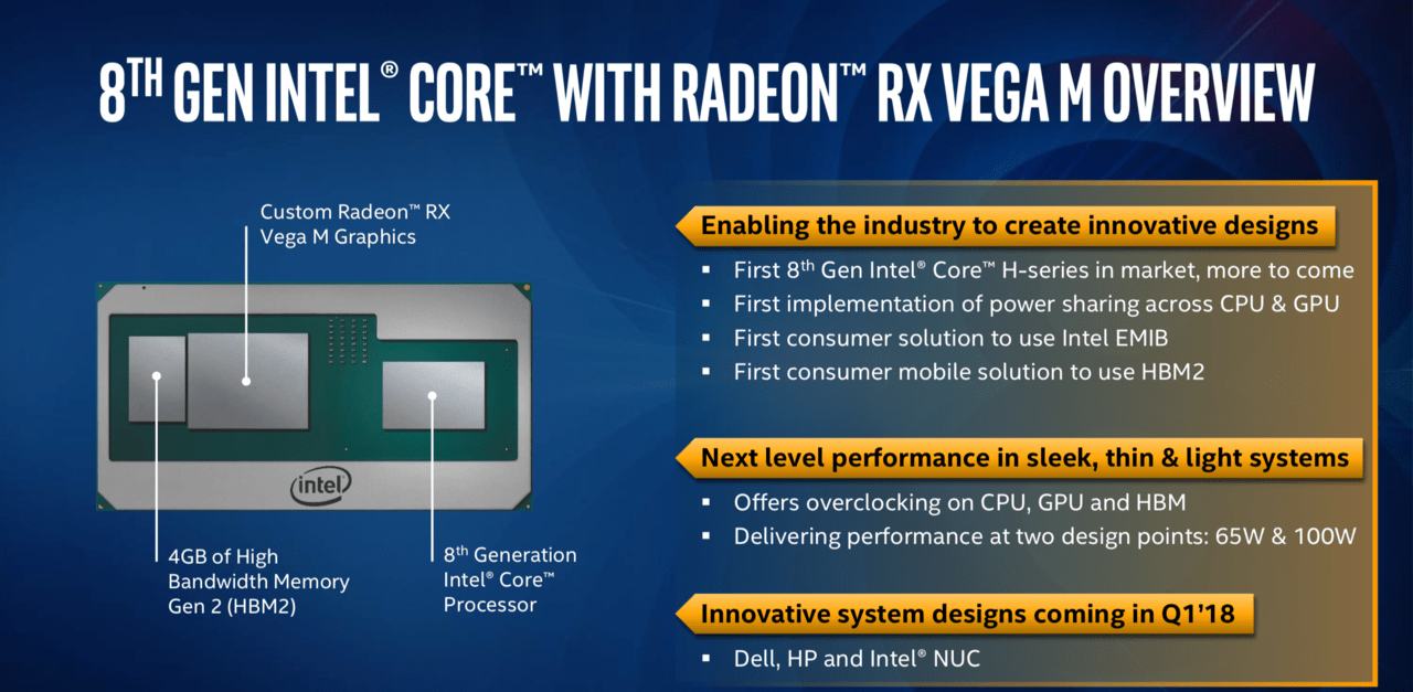
.Did KBL-G have dedicated VRAM? IIRC that was the first consumer product with EMIB to connect it to the CPU in order to use the iMC.Sounds a lot like chipset disaggregation with north- and southbridge.
The big challenge is finding a balance of following points:
Regarding the GPU the more mobile chips become chiplets based the more likely we may eventually see a return of the Kaby Lake G structure: dGPU die traditionally linked to the CPU through lean PCIe lanes, with the GPU's heavy bandwidth needs served by dedicated HBM. This allows the remaining chiplets to be optimized for latency and power efficiency without the whole product missing high performance graphics.
- For the lowest common denominator in mobile space nothing will beat monolithic.
- I/O takes a lot of space for its interfaces, this is why having those on older nodes is a good way to reduce costs.
- With SRAM something similar happens right now, with 5/4 nm apparently being the wall.
- With logic using the latest node remains the best way to save area and increase power efficiency.
- The more data is being transferred the more power wise costly it is to move that data between disaggregated chips.
In any case I'm really looking forward to seeing how exactly AMD and Intel are going to approach all these conundrums.
Definitely possible but KBL G package was huge 😅Regarding the GPU the more mobile chips become chiplets based the more likely we may eventually see a return of the Kaby Lake G structure: dGPU die traditionally linked to the CPU through lean PCIe lanes, with the GPU's heavy bandwidth needs served by dedicated HBM. This allows the remaining chiplets to be optimized for latency and power efficiency without the whole product missing high performance graphics.
Ye I would expect a laptop friendly chip based on Granite RIdge if Dragon Range has enough market penetration to be worth the resources.I disagree
At the very least, I don't think the main STX die is disaggregated. The one that would replace Phoenix/Rembrandt designs. I would not be surprised if we see another halo product like Dragon Range that is though.
For years they still optimized critical paths 'manually'. I thought they stopped doing that - but I don't really know. They could be writing optimized macros/logic blocks, typically those get re-used allot so it could be worth it.I was always under the impression that Intel does a lot of manual optimization compared to the competition.
And the way their core and uncore layouts keep looking so similar gen over gen makes me think that didn't change much even today. In any case every competitor more or less extremely lets AI optimize layout at least within but often also beyond IP blocks. The die shots of Intel CPUs on the other hand look incredible clean to this day.I was always under the impression that Intel does a lot of manual optimization compared to the competition.
That's wrong actually. The silly part about KBL-G is that EMIB was used to connect the Vega die with HBM, the CPU is still linked with traditional PCIe lanes. It's nothing more than a CPU and a traditional dGPU on a single package.IIRC that was the first consumer product with EMIB to connect it to the CPU in order to use the iMC.
Ah, thanks for the refresher. Makes much more sense indeed.And the way their core and uncore layouts keep looking so similar gen over gen makes me think that didn't change much even today. In any case every competitor more or less extremely lets AI optimize layout at least within but often also beyond IP blocks. The die shots of Intel CPUs on the other hand look incredible clean to this day.
That's wrong actually. The silly part about KBL-G is that EMIB was used to connect the Vega die with HBM, the CPU is still linked with traditional PCIe lanes. It's nothing more than a CPU and a traditional dGPU on a single package.
Yes, that's what I was responding to. You can't use average density over a very different mix of IPs to represent the difference between two particular subsystems.Dd you read what he said..?....
There s 25 bn transistors including everything, low and high density parts, and the whole amount to 140M transistors/mm2.
I obviously can't discuss the specific library details, lest I get a knock on the door from men in suits, but I'm not talking just about manual layout. If you ever find out the details of the FinFlex libraries, some of the challenges are pretty immediately apparent.What are the specific issues you see, do you guys have lots of manual stuffs in your physical design flows, timings, physical layout, floor plan, routing etc.
At least for us once specific cells for the PDK has been customized (which I doubt if at all we are doing something with it) our favorite tool can do much of the rest automatically for each macro.
However, we are on a much older node.
I think every major player does at least a bit of hand-tuning after final synthesis. At a certain point, you've basically wrung what you can out of the tools, and it's more effective to tidy up any remaining bits and pieces manually. And of course, if you want to do bug fixes without a full respin, you often have to do them by hand. Though I admittedly might be somewhat out of date here.Aside from floor-plan layouts (need IO ports on this side, need DRAM interface on this side, etc) - I would doubt anything is hand tuned. Just block level logic and cache optimized for high performance and then the Cadence/Synopsis servers go Brrrrrrr.
Sounds like Apple. Tbh, some of the macros you can get from TSMC and even Cadence/Synopsis are really not great. It's far from unheard of for big enough companies to design their own in-house. Don't know specifics for each company, but I'd be very surprised if Apple and Nvidia (at minimum) aren't doing so. AMD I only leave out as a question of historical budgeting constraints, and Intel's a mystery given their weird fab situation.According to rumors apparently some company is tinkering with their macros/IP blocks by hand heavily
But for the rest I would assume you submit your IP block designed using whichever specific cells and the final GDS is all good, because regardless of the fin type should be OK if same DRM and PDK applies.
Through Redwood Cove, Intel's big cores are very heavily hand-drawn. Supposedly part of the issue they've faced with porting between processes. I think this one of the major changes they're making with Lion Cove, but don't quote me on it. Atom seems to be far more typical.I was always under the impression that Intel does a lot of manual optimization compared to the competition.
If AMD is playing with 2 different CPU cores in Strix Point, then I would expect more cores than 8, 16(8+8) would be great.I hope for 12core chiplet for Zen5. If there will be 24core chip and stick to same clocks as Zen4, that will be the one i replace my 7950x with in the future.