EUV is expensive because there is a mountain of R&D expenses that have been invested into EUV and those expenses must be recaptured in the sale of the tools.
Sell only 10 tools and they will cost you $500m each, sell 100 tools and they might only cost you $100m each.
It is the exact same market economics at work which result in $2B stealth planes and so forth. The cost to produce the widget is not simply the production cost, you have to recapture the development cost.
Which means the question is not "what makes EUV so expensive?"; rather, the question one really means to ask is "what makes EUV
development so expensive?"
And the answer to that comes down to the customer's requirements on the tool's capabilities. Wafer throughput, defectivity, lifetime reliability, etc.
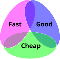
In other words, we are right back to the unavoidable consequences of the math that are captured by the
Project Management Triangle.
^ you can pick any 2 of the 3, but no more than 2.
The customers want all 3, naturally. But when asked to prioritize them they all insist on EUV being fast (competitive wafer throughput) and good (competitive defectivity, alignment, etc) and that means "cheap" is not happening at time-zero.
Cheap will happen, as more tools are sold over time the price per unit will decrease as EUV tool makers (ASML) recapture a higher and higher percentage of their development costs.
It is very similar to what makes the first few ten thousand 28nm wafers at TSMC cost $7k, but now a year later they only cost $2.5k.