Question What's going on with Power?

NTMBK

Lifer
Nov 14, 2011
10,237
5,020
136
Semiaccurate have a paywalled story up about Power: https://www.semiaccurate.com/2020/06/03/is-ibm-killing-off-power/ Apparently something big is happening, though it's definitely not being killed. Anyone got any ideas what it might be? Random thoughts that occur to me are

  • They could be selling the business
  • They could be switching fab (ditching Samsung/GloFo and going to TSMC or Intel)
  • They could be changing business model (leaning more into OpenPOWER? Killing OpenPOWER?)
Or something else entirely!
 

moinmoin

Diamond Member
Jun 1, 2017
4,952
7,661
136
Since IBM bought Red Hat I hope they make Power fit better with their whole open source strategy. That and a bigger, more public push for Power in general would be nice to have.
 

ksec

Senior member
Mar 5, 2010
420
117
116
IF they want to stay relevant, they need to get with a leading edge foundry. GloFo isn't that anymore...

Well they switched to Samsung which is what leads to the 1 year delay in POWER10.

Microwatts demonstrate what the ISA in its simplest form is capable of, and since POWER is actually well supported I thought it might take off. But then it seems the industry and market has chosen ARM.


LightningZ71

Golden Member
Mar 10, 2017
1,627
1,898
136
Power is a great architecture for its target audience. Unfortunately, their target audience is both shrinking and finding that alternative solutions are just as cost effective and capable of performing the needed tasks. There are still a few areas where there are hold outs that are tightly targeted at Power, but, I really can't see it being in any way relevant in five years.
 

NTMBK

Lifer
Nov 14, 2011
10,237
5,020
136
Power is a great architecture for its target audience. Unfortunately, their target audience is both shrinking and finding that alternative solutions are just as cost effective and capable of performing the needed tasks. There are still a few areas where there are hold outs that are tightly targeted at Power, but, I really can't see it being in any way relevant in five years.

Yeah, it feels like it's on its way out. OpenPOWER doesn't really seem to have gone anywhere- I think they were hoping the hyperscalers would take it up, but they all seem to be buying into ARM servers instead. But the article claims that "even the far future" projects are still on the roadmap, so it doesn't sound like IBM are letting it fade away just yet. All very mysterious.
 

LightningZ71

Golden Member
Mar 10, 2017
1,627
1,898
136
Look at it like this, if you are willing to target your application at Power, it means that you've likely got the ability to target most any architecture that you want. If that's the case, why would you continue to leave yourself in a single vendor lock in situation? You could decide to change to targeting ARM, which is another RISCy architecture, that has several vendors dumping a lot of money into it and developing high reliability, high performance solutions for the server space. Aside from a scarce few exclusive features, Power just isn't bringing anything unique to the table. All they are effectively doing is providing updated systems to support legacy Power code for situations where a company needs better performance but doesn't want to switch software or redevelop it for a new architecture. In essence, it's where COBOL was about a decade ago to use a loose analogy. Eventually, all of that code will be replaced with something more modern.
 

Gideon

Golden Member
Nov 27, 2007
1,641
3,678
136
Well it looks that Samsung 7nm actually can fab large chips (finally). Power 10 released:


Specs from Anderas Schilling
  • 602 mm² die size
  • 18 Billion transistors
  • 16 cores (15 active) per die
  • SMT4/SMT8 -
  • 48/32 L1-Cache (I/D)
  • 2 MB L2-Cache
  • 128 MB L3-Cache
  • Single Chip Module (SCM) / Dual Chip Module (DCM)

IBM-POWER10-Press-Conference-Deck-009_E10C95C1A63F4C989B4F3F20AC434A0B.jpg
 

NostaSeronx

Diamond Member
Sep 18, 2011
3,686
1,221
136
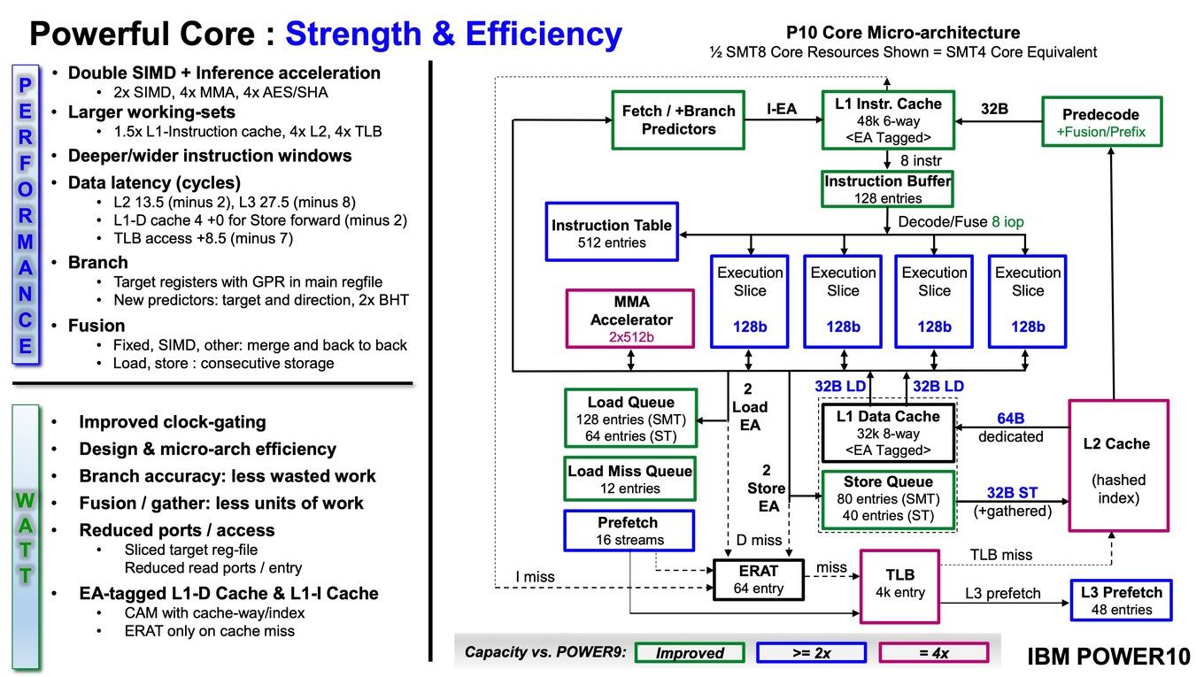
Seems they improved the CMT granularity.

POWER9 splits into two independent blocks w/ up to 1-4 threads being processed per.
POWER10 splits into four independent blocks with up to 1-2 threads being processed per.

Won't be surprised if they launch a 64/128 SMT2-core version.
 
Last edited:

NTMBK

Lifer
Nov 14, 2011
10,237
5,020
136
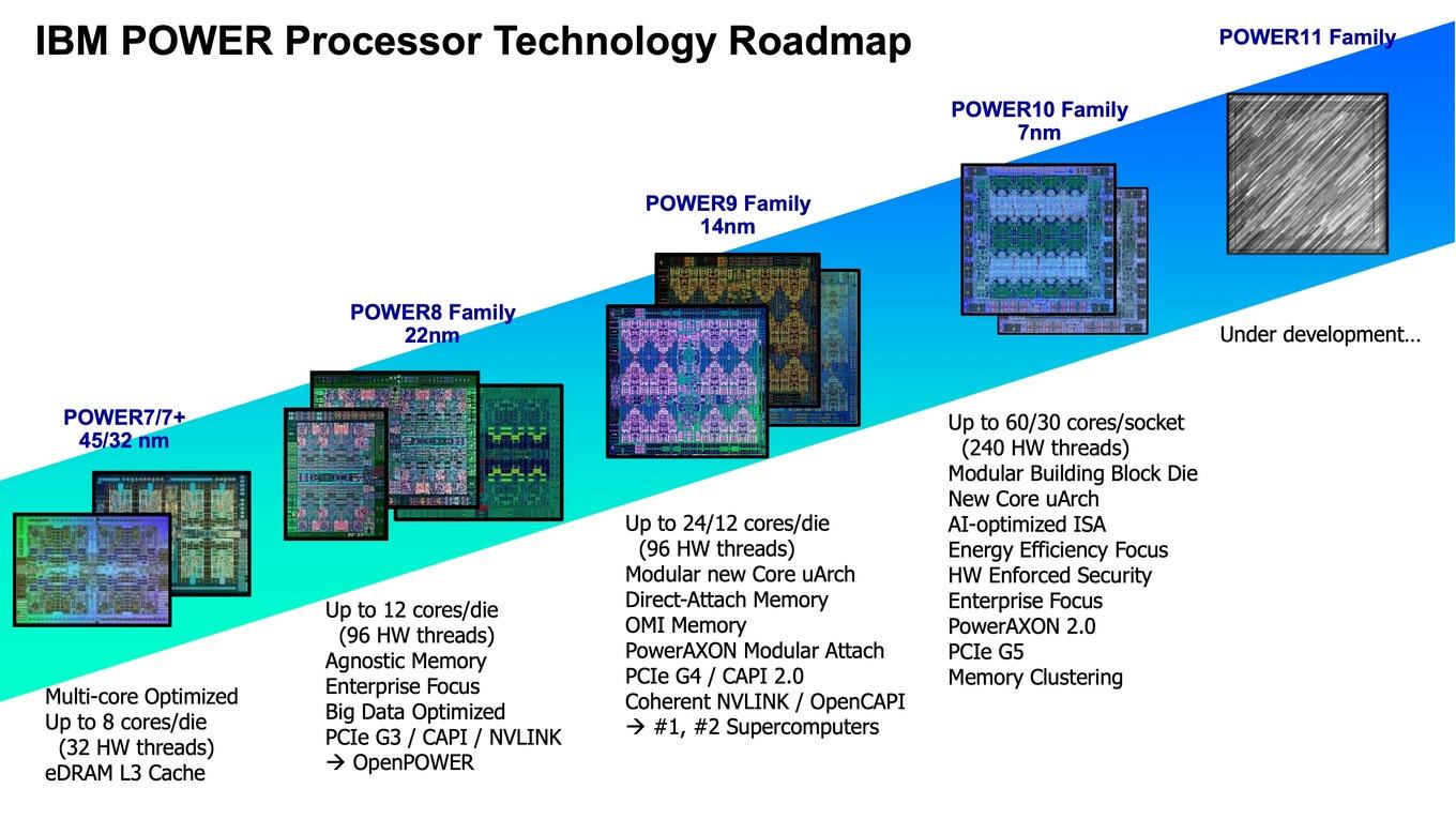
And POWER11 is officially "in development":

IBM-POWER10-Press-Conference-Deck-006_C66EE6D667E6488D8448250EBFF24B8C.jpg


Nice to see POWER10 come out! Interestingly they only sell up to 15 enabled cores- sounds like they're struggling with yield a bit.

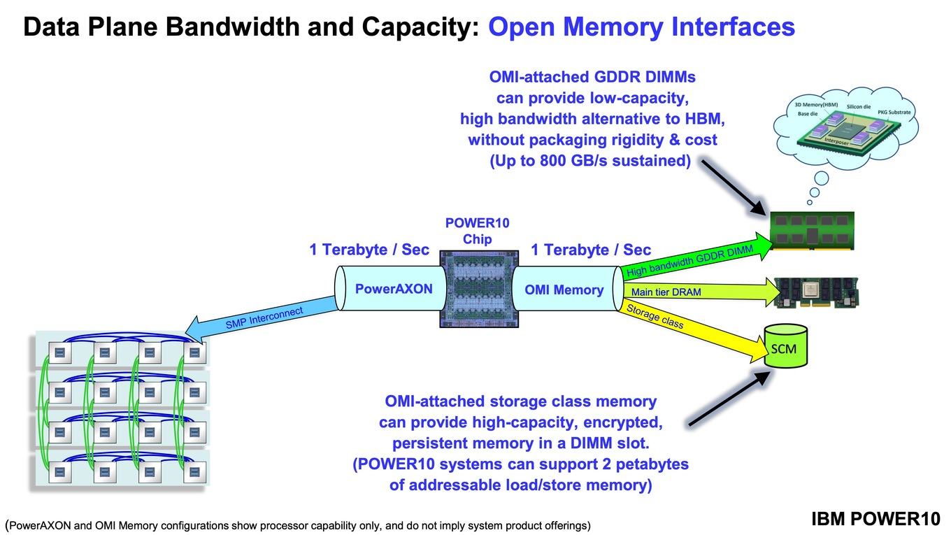
Also interesting- GDDR DIMMS!

IBM-POWER10-Press-Conference-Deck-013_E94851F69D344B0D8918DE4CDE964F3E.jpg


Equally interesting- their slides call out "FPGAs and ASICs" as attached accelerators, but no mention of GPUs. Between that and the new focus on CPU AI performance, is the partnership with NVidia dead?
 
  • Like
Reactions: coercitiv

DrMrLordX

Lifer
Apr 27, 2000
21,632
10,845
136
Also interesting- GDDR DIMMS!

Weird. They're using the same interface to connect to DRAM, GDDR DRAM, and storage? Simultaneously? Sounds like they're trying to do something Optane-like but without Optane.

Equally interesting- their slides call out "FPGAs and ASICs" as attached accelerators, but no mention of GPUs. Between that and the new focus on CPU AI performance, is the partnership with NVidia dead?

Maybe. I think they're trying to emphasize OpenCAPI which, to date, hasn't exactly had a blinding array of products available to utilize the interface. Even nVidia never used it (POWER9 systems like Summit used NVLink).
 

moinmoin

Diamond Member
Jun 1, 2017
4,952
7,661
136
Weird. They're using the same interface to connect to DRAM, GDDR DRAM, and storage? Simultaneously? Sounds like they're trying to do something Optane-like but without Optane.
I think that's not necessarily like Optane (which is storage tier masking itself as slow memory) but more like AMD's SerDes/PCIe PHY that is agnostic enough to simultaneously support further SATA and USB connections in place of lanes.

Though going by the slide I'd expect further logic to be necessary to actually connect all the tiers, and it comes with the caveat of additional latency that likely wouldn't fly on the desktop:
- Technology agnostic: near/main/storage tiers
- Minimal (< 10ns latency) add vs DDR direct attach
 

Jimzz

Diamond Member
Oct 23, 2012
4,399
190
106
Yea my thought is they are going to spin it off or try and sell. My buddy has told me a lot of POWER engineering positions are not being back filled. That and some other things going on inside as well.
 

KompuKare

Golden Member
Jul 28, 2009
1,015
930
136
If I'm reading this correctly that's a huge density difference between this with its
18 billion transistors in 602mm²
and Renoir with its
9.8 billion transistors in 156mm²
Is that explainable just by the differences in density between cache, iGPU and so on, or IBM traded density for speed?
 

Markfw

Moderator Emeritus, Elite Member
May 16, 2002
25,560
14,514
136
If I'm reading this correctly that's a huge density difference between this with its
18 billion transistors in 602mm²
and Renoir with its
9.8 billion transistors in 156mm²
Is that explainable just by the differences in density between cache, iGPU and so on, or IBM traded density for speed?
Looks like 2x the density for TSMC ... Not that good for samsung....
 

Jimzz

Diamond Member
Oct 23, 2012
4,399
190
106
If I'm reading this correctly that's a huge density difference between this with its
18 billion transistors in 602mm²
and Renoir with its
9.8 billion transistors in 156mm²
Is that explainable just by the differences in density between cache, iGPU and so on, or IBM traded density for speed?

Renior is half the CPUs, a LOT less cache, PCIe 3.0 vs 5.0, memory channels, etc...

I still think TSMCs 7nm is probably better than Samsungs in this area as well but many different things going on in those 2.
 

Markfw

Moderator Emeritus, Elite Member
May 16, 2002
25,560
14,514
136
Renior is half the CPUs, a LOT less cache, PCIe 3.0 vs 5.0, etc...

I still think TSMCs 7nm is probably better than Samsungs in this area as well but many different things going on in those 2.
If you multiply 156*4 you get 624 or very close to the 602 number in size, but that would enable 9.8*4 b transistors or almost 40 billion, or twice the samsung density.
 

JasonLD

Senior member
Aug 22, 2017
485
445
136
Looks like 2x the density for TSMC ... Not that good for samsung....

Power9 had 8B transistor count on 14nm GF process with the die size of 693.37 mm². While each Zen 1 chiplet had 4.8B transistor count with the die size of 212.97 mm² using same process.
I think it has more to do with Power architecture's design choice of using relaxed density (For clockspeed and heat?) rather than the density of Samsung's 7nm itself.
 
Last edited:

Markfw

Moderator Emeritus, Elite Member
May 16, 2002
25,560
14,514
136
Power9 had 8B transistor count on 14nm GF process with the die size of 693.37 mm². While each Zen 1 chiplet had 4.8B transistor count with the die size of 212.97 mm² using same process.
I think it has more to do with Power architecture's design choice of using relaxed density (For clockspeed and heat?) rather than the density of Samsung's 7nm itself.
I don't pretend I know the details, I was just doing the math.
 

thetrashcan

Junior Member
Jan 13, 2020
4
16
41
If I'm reading this correctly that's a huge density difference between this with its
18 billion transistors in 602mm²
and Renoir with its
9.8 billion transistors in 156mm²
Is that explainable just by the differences in density between cache, iGPU and so on, or IBM traded density for speed?

I think there are a couple of contributing factors to the lower density, beyond process differences between TSMC and Samsung 7nm and relaxed design rules to allow for higher clock speeds. To be clear, I suspect that a large part of the density differences are the result of process differences, but we also need to consider that large portions of the Power10 die are made up of structures that are not typically very transistor dense - or "device" dense, to use IBM's terminology, since I believe they are including capacitors and transistors in their device count (because of eDRAM).

1. I/O
IBM has a truly immense amount of off-chip I/O with Power10 - overall, we are looking at 304 SerDes operating at up to 32GT/s (16x8 OMI + 4x(32+4) PowerAXON + 2x16 PCIe5). This occupies the entire perimeter of the chip and accounts for around ~185 mm² (~30% of the die size). Off-chip I/O is known to scale poorly with process improvements - in fact, that is why the I/O die of AMD's Rome is made on GF 12nm, rather than TSMC 7nm.

2. eDRAM
IBM is still using eDRAM for it's L3, which skews things slightly - eDRAM is 2 "devices" per bit, one transistor and one capacitor, compared to SRAM, which is 6(+) transitors per bit. IIRC eDRAM has historically been less device-dense than SRAM because the capacitors are larger than transistors - though overall it is still smaller on a per-bit basis. IBM is still achieving ~9.1Mb/mm² with its eDRAM L3, compared to 7.6Mb/mm² for the SRAM L3 on the Rome CCD; not a super useful comparison, since they are on different processes, but it does illustrates that eDRAM has density advantages.

The cache regions appear to account for ~112mm² (~19% of the die), which includes 2.15B devices (2^30 bits * 2 devices) for the cache bits, plus some percentage for whatever ECC scheme has been implemented, plus whatever is necessary for the eDRAM control and on-chip network. So the remaining ~490mm² accounts for <15.85B devices, which puts the remaining die at <32.3M devices per mm², rather than the 29.9M devices per mm² assumed initially - presumably the vast majority of these remaining devices (if not all of them) are transistors and not capacitors, since we are excluding eDRAM.
 
Last edited: