
Blitzvogel
Platinum Member
- Oct 17, 2010
- 2,012
- 23
- 81
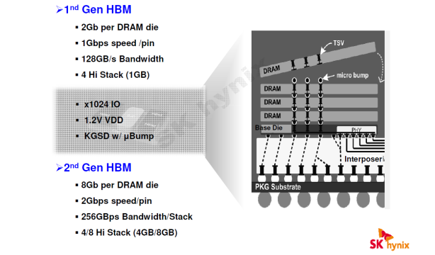
In 2017 for the first Zen laptop APU, with second generation HBM I am thinking AMD could probably get by with one stack of HBM (which would be either 2GB/4GB/8GB in capacity depending on the size of the dram die and how high the stack is) with 128GB/s bandwidth @ 1Gbps per pin and 256 GB/s @ 2Gbps per pin available for bandwidth.
128 GB/s is a lot of bandwidth considering I would expect a 35W laptop chip with 1024sp to be clocked pretty low.
For 1024 SPs in the 1 GHz region, I don't think 128 GB/s is enough unless there are major changes to GCN architecture like increased cache and continued progress on data and color compression like with Nvidia Maxwell. I'm also a bit skeptical on the cost of HBM coming down quickly, so it may be more conducive to use two stacks of 4 x 2 Gb instead of 4 x 4 Gb. Might as well spread the love of an 8 x 2 Gb. It also should the heat around, and if the die is produced with 2 HBM connection pads, I don't see the issue in letting the customer decide if they want something that uses just one pad or not.
Now, I'm not completely versed on HBM, are all the chips in the stack the exact same or are there slight variations in each module to supply power and data to the chips above it in the stack?