
What will be the die size of the Orochi Bulldozer?
- Thread starter cbn
- Start date
You are using an out of date browser. It may not display this or other websites correctly.
You should upgrade or use an alternative browser.
You should upgrade or use an alternative browser.
Voted 176-225mm^2.
From what we know of BD...if it were built on the existing 45nm process I wouldn't expect the core-logic area for 4 modules to be all that much larger than the core logic area for the 6 logic cores of a Thuban.
Take that and shrink its die area thanks to 32nm. It gets smaller than thuban. Add in more cache than what thuban has and it grows a little.
Frankly I'd be surprised if an 8-core bulldozer (4 module) with all the extra cache is any larger than an X4 Phenom II in 45nm process. (258mm^2)
But I want to be optimistic, so I voted that it would <225mm^2")
From what we know of BD...if it were built on the existing 45nm process I wouldn't expect the core-logic area for 4 modules to be all that much larger than the core logic area for the 6 logic cores of a Thuban.
Take that and shrink its die area thanks to 32nm. It gets smaller than thuban. Add in more cache than what thuban has and it grows a little.
Frankly I'd be surprised if an 8-core bulldozer (4 module) with all the extra cache is any larger than an X4 Phenom II in 45nm process. (258mm^2)
But I want to be optimistic, so I voted that it would <225mm^2
- Mar 27, 2009
- 12,968
- 221
- 106
Does anyone have ideas on how faster clockspeeds/Higher Ghz would impact xtor size and thus die size for Bulldozer?
Do faster xtors need to be larger?
Thank you for the vote. For anyone else contemplating on voting please notice I set the poll to anonymous.
Do faster xtors need to be larger?
Awesome, I voted the same as IDC without reading, I feel good about myself.
Thank you for the vote. For anyone else contemplating on voting please notice I set the poll to anonymous.
Does anyone have ideas on how faster clockspeeds/Higher Ghz would impact xtor size and thus die size for Bulldozer?
Do faster xtors need to be larger?
Thank you for the vote. For anyone else contemplating on voting please notice I set the poll to anonymous.
switching speed has a rollover point versus xtor length so there will be a minimum length for which the switching time is also a minimum (what we laymen think of as a transistor "width" from all those fancy SEM cross-sections is actually the length of a xtor, the width runs perpendicular).
The question you are asking though is really quite complicated if you aren't familiar with circuit design.
I'd love to see Ctho9305 or TuxDave break it down for the general audience, take it away fella's! :thumbsup:
ModestGamer
Banned
- Jun 30, 2010
- 1,140
- 0
- 0
I don't think you can figure out anything useful with this line of reasoning. However, I find the relationship between sizing and area to be an interesting topic, so if you ask questions, I will try to answer them.switching speed has a rollover point versus xtor length so there will be a minimum length for which the switching time is also a minimum (what we laymen think of as a transistor "width" from all those fancy SEM cross-sections is actually the length of a xtor, the width runs perpendicular).Does anyone have ideas on how faster clockspeeds/Higher Ghz would impact xtor size and thus die size for Bulldozer?
Do faster xtors need to be larger?
The question you are asking though is really quite complicated if you aren't familiar with circuit design.
I'd love to see Ctho9305 or TuxDave break it down for the general audience, take it away fella's! :thumbsup:
As for why you can't go anywhere from here: you could build an 800MHz ARM Cortex A9 and a 2GHz one, and the 2GHz one will be bigger (6.7mm^2 vs 4.6mm^2 on TSMC 40G)... but they're the same microarchitecture. You could probably use pretty small gates on a design like Intel's canceled Tejas and still end up with a very high frequency (<10 gates in a cycle), while you'll never get much speed even with arbitrary large gates if you're building an Intel 80386 clone (I vaguely remember learning that it had something like 80 gates in a cycle).
ARM's marketing information for their standard cell libraries might have some interesting tidbits to prompt more questions, but I haven't read through it myself.
Skolomerija
Junior Member
- Sep 6, 2010
- 9
- 0
- 0
Welcome to the forums Skolomerija!
The quick answer to your question is that yes, absolutely, it is possible.
The process is called chip-stacking and it happens already in the flash industry and set to become the standard required for producing the ram densities needed for DDR4 in another 2 yrs.
The challenge with stacking L3$ is of course the speed - stacking doesn't make the stacked chips any faster just because they are stacked - and the heat dissipation.
Intel has been public about there work in the area of chip stacking with cpu's and they have concluded that at this point in time the benefits do not outweigh the downsides so they aren't planning to implement this.
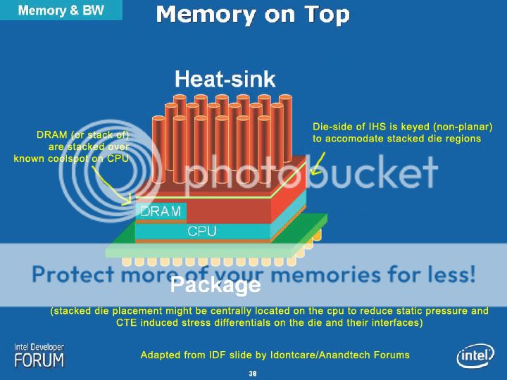
For more discussion see this thread.
The quick answer to your question is that yes, absolutely, it is possible.
The process is called chip-stacking and it happens already in the flash industry and set to become the standard required for producing the ram densities needed for DDR4 in another 2 yrs.
The challenge with stacking L3$ is of course the speed - stacking doesn't make the stacked chips any faster just because they are stacked - and the heat dissipation.
Intel has been public about there work in the area of chip stacking with cpu's and they have concluded that at this point in time the benefits do not outweigh the downsides so they aren't planning to implement this.
For more discussion see this thread.
- Mar 27, 2009
- 12,968
- 221
- 106
The process is called chip-stacking and it happens already in the flash industry and set to become the standard required for producing the ram densities needed for DDR4 in another 2 yrs.
With regard to the stacked DDR4 mentioned, does anyone know how much of an issue heat dissipation becomes? Would it be enough to force lower memory speeds in order to maintain reasonable component life?
With regard to the stacked DDR4 mentioned, does anyone know how much of an issue heat dissipation becomes? Would it be enough to force lower memory speeds in order to maintain reasonable component life?
You can break out your favorite text translator or brush up on your Kanji and checkout these two Goto-san articles:
http://pc.watch.impress.co.jp/docs/column/kaigai/20100823_388253.html
http://pc.watch.impress.co.jp/docs/column/kaigai/20100816_387444.html
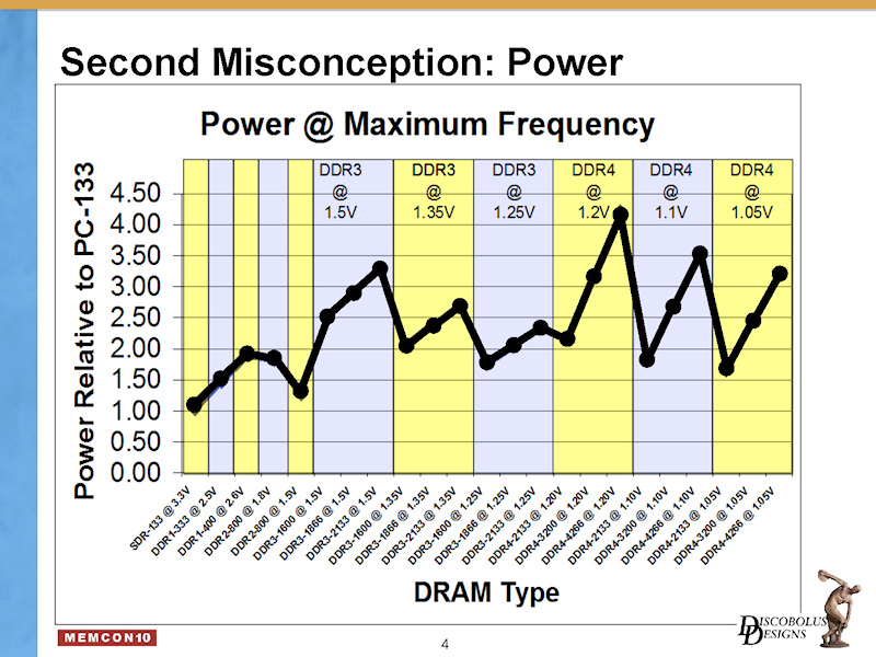
Power density is definitely going to increase. But it is low already (unless you've got 64 dimms populated
) so doubling an already small number still leaves you with a small number.~300 mm^2
I think some people are forgetting about all the "uncore" stuff that is needed (big L3 cache, IMC, northbridge, hypertransport links), and that the modules are each likely to come with 2MB of L2.
Either that, or they don't realize this is a 4-module/8-core die.
I think some people are forgetting about all the "uncore" stuff that is needed (big L3 cache, IMC, northbridge, hypertransport links), and that the modules are each likely to come with 2MB of L2.
Either that, or they don't realize this is a 4-module/8-core die.
ModestGamer
Banned
- Jun 30, 2010
- 1,140
- 0
- 0
~300 mm^2
I think some people are forgetting about all the "uncore" stuff that is needed (big L3 cache, IMC, northbridge, hypertransport links), and that the modules are each likely to come with 2MB of L2.
Either that, or they don't realize this is a 4-module/8-core die.
Its not a intel chip. There is alot of streamlining and resource utilization change in the architecture that make it very unlike previous products intel and AMD offered. Before we just had two slightly different flavors of koolaid. Lemonade and Pink lemonade. Now we are getting Straberry fruit juice and pink lemonade.
Skolomerija
Junior Member
- Sep 6, 2010
- 9
- 0
- 0
TRENDING THREADS
-
 Discussion Zen 5 Speculation (EPYC Turin and Strix Point/Granite Ridge - Ryzen 9000)
- Started by DisEnchantment
- Replies: 25K
-
Discussion Intel Meteor, Arrow, Lunar & Panther Lakes + WCL Discussion Threads
- Started by Tigerick
- Replies: 23K
-
 Discussion Intel current and future Lakes & Rapids thread
- Started by TheF34RChannel
- Replies: 23K
-

-

AnandTech is part of Future plc, an international media group and leading digital publisher. Visit our corporate site.
© Future Publishing Limited Quay House, The Ambury, Bath BA1 1UA. All rights reserved. England and Wales company registration number 2008885.