What SSDs are coming with 3D QLC NAND?

cbn

Lifer
Mar 27, 2009
12,968
221
106
So far:

Intel 660p---> http://www.tomshardware.com/news/intel-760p-660p-700p-specifications,36335.html

Last but not least is the most interesting leak: In the middle of the chart is the Intel SSD 660p with 4-bit per cell (QLC) flash. The SSD 660p listing shows three capacities (512GB, 1TB and 2TB). The performance is much higher than we expected to see from QLC at right out of the gate. The leak says the 660p will achieve up to 1,800 MB/s sequential read and 1,100 sequential write speeds. The random performance clocks in at 150,000 IOPS for both reads and writes.

QLC was a hot topic at CES last week, but only behind closed doors. No one wanted to go on the record, but we know IMFT (Intel Micron Flash Technology) has it ready for the most part. Companies are excited about the cost-cutting technology but need controllers to pair with it. One source told us to expect 512GB QLC SSDs for around $100.
 

VirtualLarry

No Lifer
Aug 25, 2001
56,327
10,034
126
going by the title of the second article link, do these QLC NANDs actually have 1000 effective P/E cycles? If so, I guess, bring them on! Doesn't sound horrible, although I still prefer me a nice 20nm MLC NAND any day.
 

ao_ika_red

Golden Member
Aug 11, 2016
1,679
715
136
I wonder if that Toshiba roadmap has changed since they sold their NAND business to Gain Capital (at least that was the last thing I read about them):

https://www.anandtech.com/show/1214...l-settle-disputes-over-sale-of-toshiba-memory
Because it's a very stratetegic business, the deal was overseen directy by Japan and US govt. And even though Bain capital is from the states, but majority of the consortium itself is still from Japan.
https://www3.nhk.or.jp/nhkworld/nhknewsline/backstories/toshibaofficiallysignsdeal/

And rest assured, they just announced of new investment in NAND fab last December.
http://www.tomshardware.com/news/toshiba-invests-new-nand-fab,36165.html
 

Glo.

Diamond Member
Apr 25, 2015
5,705
4,549
136
Are QLC SSDs actually viable? Do you guys think that the rumors are true, and 660p 512 GB NVMe drive will cost around 100$, and have 1000 p/e cycles lifespan?

That would be something genuinely new...
 

Glaring_Mistake

Senior member
Mar 2, 2015
310
117
116

According to Tomshardware the 860 might be the first drive from Samsung to use QLC NAND: http://www.tomshardware.com/news/samsung-850-ssd-860-evo,35675.html

However just recently the 860 Pro turned up on Samsung's website so at least the rumors of Samsung moving away from using Pro/EVO to distinguish between drives may be inaccurate.


Recently found something I think you'll find interesting: http://thememoryguy.com/how-3d-nand-shrinks-ecc-requirements/
According to this article it looks like it should be child's play to correct for errors for 3D QLC NAND compared to for 2D NAND below 20nm.
I think that that is a tad optimistic since in my tests 3D NAND has slowed down a bit faster than expected where even some SSDs with 2D NAND sub-20nm has stood up better to voltage drift.

going by the title of the second article link, do these QLC NANDs actually have 1000 effective P/E cycles? If so, I guess, bring them on! Doesn't sound horrible, although I still prefer me a nice 20nm MLC NAND any day.

Think that is possible, though if we look at the WD Blue 3D (using 3D TLC NAND) it is specified for 1000 P/E cycles despite that it should have an advantage in endurance.
But if for example they just thought 1000 P/E cycles was than sufficient for a consumer drive then their 3D TLC NAND could have higher endurance than that making it more likely that their 3D QLC NAND could have an endurance of around 1000 P/E cycles.

Don't know if consumers tend to need to think much about endurance however.

Are QLC SSDs actually viable? Do you guys think that the rumors are true, and 660p 512 GB NVMe drive will cost around 100$, and have 1000 p/e cycles lifespan?

That would be something genuinely new...

Probably, yes, maybe, could be.
 
  • Like
Reactions: cbn

cbn

Lifer
Mar 27, 2009
12,968
221
106
Recently found something I think you'll find interesting: http://thememoryguy.com/how-3d-nand-shrinks-ecc-requirements/
According to this article it looks like it should be child's play to correct for errors for 3D QLC NAND compared to for 2D NAND below 20nm.
I think that that is a tad optimistic since in my tests 3D NAND has slowed down a bit faster than expected where even some SSDs with 2D NAND sub-20nm has stood up better to voltage drift.


Yes, the author suggests LDPC for 5 bits (or more) per cell:

Over the long term I would assume that LDPC will be used in most 3D NAND controllers to allow even more than 4 bits to be stored per cell, but it may take some time to get to that point. During the near term it’s reasonable to expect for 3D NAND to largely shift to QLC using simple BCH algorithms.

But I do remember there appeared to be such a relatively large difference between the different planar TLC NANDs. (Eg, the Toshiba/Sandisk 15nm TLC seemed so much better than the 16nm SK Hynix and 16nm Micron TLC). So I wonder how large the spread will be for 3D considering there may be a larger delta?? in lithography (and/or NAND design) among the various manufacturers??
 

cbn

Lifer
Mar 27, 2009
12,968
221
106
This article mentions Samsung with a 1Tb (128GB) 3D QLC die coming what would be this year:

https://www.pcper.com/news/Storage/...-QLC-V-NAND-16TB-NGSFF-SSD-Z-SSD-V2-Key-Value

The arrival of a 1Tb V-NAND chip next year will enable 2TB of memory in a single V-NAND package by stacking 16 1Tb dies and will represent one of the most important memory advances of the past decade.

For Samung 860 EVO?

Or something else?

If Samsung 860 EVO is offered in 256GB capacity that would only be two dies.
 
Last edited:

Glo.

Diamond Member
Apr 25, 2015
5,705
4,549
136
For Samung 860 EVO?

Or something else?

If Samsung 860 EVO is offered in 256GB capacity that would only be two dies.
Isn't 860 Evo just 128 Gbit TLC dies?

Its also important from price perspective, that M.2 2280 SSDs from that line start at 500 GB capacity, which may suggest that the capacity/price point has shifted. Which also would suggest that we are looking at new NAND technology.
 

Glo.

Diamond Member
Apr 25, 2015
5,705
4,549
136
Guys, what technology will this year bring to the table of NAND?

850 Evo was using 128 Gb TLC V-NAND, that was made in 40(!) nm process. Shouldn't we be currently on much smaller nodes for NAND flash?
 

Charlie22911

Senior member
Mar 19, 2005
614
228
116
I think for the average user endurance on these will be fine. I still own every SSD I’ve ever purchased over the years (12) and the only one that’s died was a 950pro, which I believe was the fault of the controller and not NAND.
 

cbn

Lifer
Mar 27, 2009
12,968
221
106
Isn't 860 Evo just 128 Gbit TLC dies?

Here is a quote from the first link in post #7:

Samsung 860 Series 256GB, 500GB, 1TB, 2TB, And 4TB

aHR0cDovL21lZGlhLmJlc3RvZm1pY3JvLmNvbS9JL1kvNzIyNTU0L29yaWdpbmFsLzg2MF9FVk8uanBn

We also found a reference to the upcoming Samsung 860 series. This came from the SATA-IO Integrators List that was updated on September 27 with the drive. The list refers to the drive as the 860 EVO, and that goes against the story of Samsung moving away from the EVO / Pro names.

The list shows five capacities for this series, 256GB, 500GB, 1TB, 2TB, and 4TB. All of those sizes were used in the 850 EVO, so you wouldn't assume these offer anything special except a controller and NAND update to 64-layers. That might be true, but later in the evening we spoke with an insider who led us down a different path: We were told to expect the Samsung 860 to be the company's first consumer QLC SSD.

If our information is accurate, the next generation EVO products could represent QLC technology and the non-EVO models could be code for TLC. At this point it's all speculation, but that's what makes being the cat more fun than being the mouse.

So if that ends up being right EVO would be 3D QLC.
 

Glaring_Mistake

Senior member
Mar 2, 2015
310
117
116
Yes, the author suggests LDPC for 5 bits (or more) per cell:


But I do remember there appeared to be such a relatively large difference between the different planar TLC NANDs. (Eg, the Toshiba/Sandisk 15nm TLC seemed so much better than the 16nm SK Hynix and 16nm Micron TLC). So I wonder how large the spread will be for 3D considering there may be a larger delta?? in lithography (and/or NAND design) among the various manufacturers??

Noticed that too but the trend has been going over to using LDPC for 3D TLC NAND and planning to use some fairly strong ECC (like various versions of LDPC or QSBC) for 3D QLC NAND.
So I don't know how likely it is that they go back to using BCH ECC again.

About why I'm not sure that 3D NAND has such a huge advantage in retention over 2D NAND as The Memory Guy claims; did you want to see the reason why?


Yes, according to my tests Toshiba/SanDisk 15nm TLC is a bit more resistant to voltage drift than 16nm TLC NAND by either Intel/Micron or SK Hynix.
How well Samsung's 16nm TLC NAND does in comparison is difficult to determine but I think it may be somewhere in between those two groups.
But it is difficult to say for certain if any difference between the different drives may be at least partly down to the controller/firmware.


About the difference in lithography it may be that the IMFT 3D NAND uses a 16-20nm lithography but at the same time that is not the whole truth.
Found this in an article from a Flash Memory Summit about 3D NAND:
"Geometry terms like 40nm or 20nm are not useful. Architecture is too complex for analysis like this.
• All companies have channel holes at 60nm+ and contacts at 20nm
• Vertical gate spaces and features can be <20nm"

Don't know why they would call it 16-20nm if it is just one of the measurements however.

Guys, what technology will this year bring to the table of NAND?

850 Evo was using 128 Gb TLC V-NAND, that was made in 40(!) nm process. Shouldn't we be currently on much smaller nodes for NAND flash?

Transitioning from 2D NAND to 3D NAND allowed manufacturers to use a larger node and to increase capacity by stacking more and more layers.
So you should look forward to increased amount of layers rather than nodes dropping in size.

Here is a quote from the first link in post #7:
So if that ends up being right EVO would be 3D QLC.

It is possible that with the 860 Pro and EVO the Pro is going to use 3D TLC NAND instead of 3D MLC NAND and that the 860 EVO 3D QLC NAND instead of 3D TLC NAND.
Though so far we've only seen that the 860 Pro/EVO is going to arrive but not what NAND they're using.
 
  • Like
Reactions: cbn

cbn

Lifer
Mar 27, 2009
12,968
221
106
It is possible that with the 860 Pro and EVO the Pro is going to use 3D TLC NAND instead of 3D MLC NAND and that the 860 EVO 3D QLC NAND instead of 3D TLC NAND.
Though so far we've only seen that the 860 Pro/EVO is going to arrive but not what NAND they're using.

Or maybe could it be 860 Pro is 3D MLC, 860 EVO is 3D TLC and 860 is 3D QLC?
 

IntelUser2000

Elite Member
Oct 14, 2003
8,686
3,785
136
850 Evo was using 128 Gb TLC V-NAND, that was made in 40(!) nm process. Shouldn't we be currently on much smaller nodes for NAND flash?

No. 40nm is about the point where number of write cycles started degrading significantly. 3D NAND allows manufacturers to use the older, better nodes, while having better density due to having many layers of them.

Don't know why they would call it 16-20nm if it is just one of the measurements however.

Same reason that they call it "Dell XPS 13 2017", rather than Dell XPS 1.1x. At one point, there was a rough correlation between node naming and sizes, but that changed. Since node advances bring a certain expected advantage, they call the new one whatever they want as long as it brings the expected benefits.

Say there are two 25nm nodes:

First one is a true 25nm node, with smallest feature size being 25nm. Say the density is 2x 40nm.

Second one is just called 25nm node, but smallest feature size is much larger. The density is still 2x 40nm.

Practically speaking, they are both 25nm, because they bring 2x the advantage in density. It used to be nodes were named by Gate Length. Since that isn't the factor in determining density of a node, it doesn't matter if the Gate Length no longer corresponds to the node naming.
 

Glaring_Mistake

Senior member
Mar 2, 2015
310
117
116
Same reason that they call it "Dell XPS 13 2017", rather than Dell XPS 1.1x. At one point, there was a rough correlation between node naming and sizes, but that changed. Since node advances bring a certain expected advantage, they call the new one whatever they want as long as it brings the expected benefits.

They don't include the lithography in the specifications for their 3D TLC NAND however so why choose to say that their 3D MLC NAND is using a 16-20nm lithography if they're reluctant from doing the same with their 3D TLC NAND?


Or maybe could it be 860 Pro is 3D MLC, 860 EVO is 3D TLC and 860 is 3D QLC?

That's fairly likely too.
It's just that I haven't heard about Samsung making 64-layer 3D MLC NAND and the 860 EVO and Pro have been confirmed but not 860 which made me think that the Pro might use 3D TLC NAND and the 860 EVO 3D QLC NAND.

Regardless which one is accurate I think the naming has become a bit odd since the new 850 which uses 3D TLC NAND would be below the drive using 3D QLC NAND.

Yes. Most definitely!

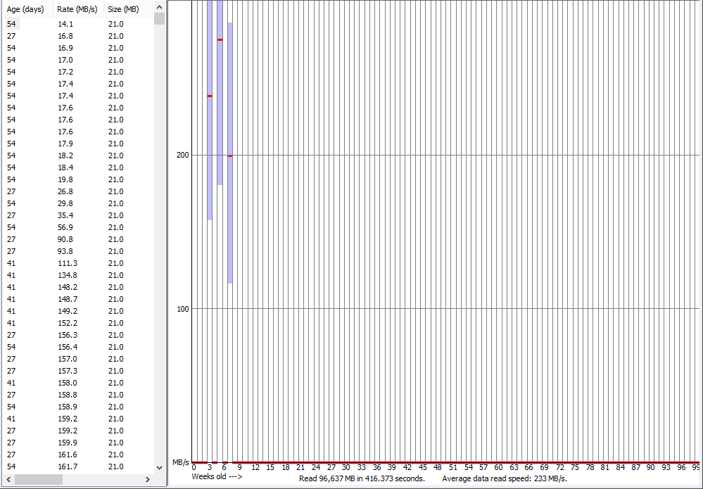
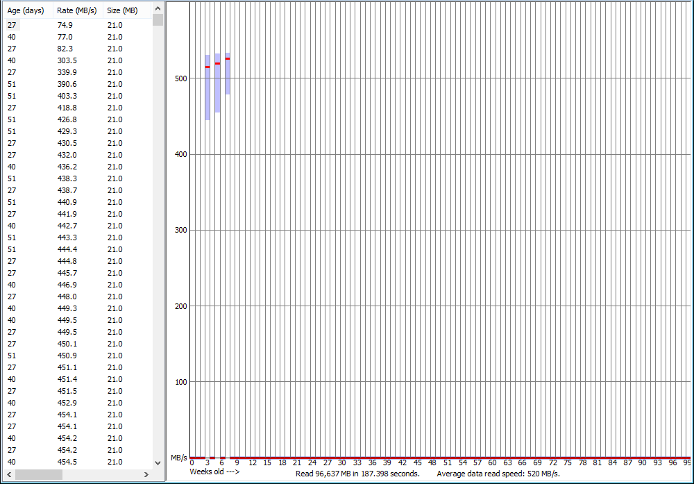
Ok, so here's two tests with two different drives with one using 3D TLC NAND and one using 2D sub-20nm MLC NAND (but not saying which ones yet to so as not to spoil too much for when I finally write something a bit more extensive on them):

20170623212321Result.png


20170903171746Result.png


Now, if I were to tell you that the first one uses 3D TLC NAND and the second one uses 2D sub-20nm MLC NAND would you be very impressed with how well the drive using 3D TLC NAND manages to keep voltage drift under control?
 

Glaring_Mistake

Senior member
Mar 2, 2015
310
117
116
Some new information on things we've discussed from Techreport:

"Samsung's stacks of flash have tripled in height since then—the company recently announced its forthcoming fifth-generation, 96-layer V-NAND. That flash may mark the end of line for Samsung's layer jenga. The company has hinted it will likely be seeking future gains through means other than adding more layers."

If I recall correctly Samsung has said previously that they intend to scale up to at least 128 layers so it sounds a bit odd to hear that.
Though Samsung also said that they would not make 3D QLC NAND and that 3D TLC NAND was the future just months before they cheerfully announced they were going to make 3D QLC NAND.
So it may be good to take what Samsung says with a pinch of salt.


"Claims like "2x performance" and "PCIe performance at near SATA pricing" abound. So whence come all these savings? Intel would have us believe it all comes down to foresight. Pursuing traditional floating-gate arrays in its 3D NAND product allowed IMFT to preserve smaller cell sizes where its charge-trap competitors were forced to go bigger, reducing density. "

Sounds like this strengthens the case for their 3D NAND being built on more like a 16-20nm lithography (as Intel states for some of their drives using 3D MLC NAND) than a larger one like Samsung's.
It's odd though that I've heard several different estimations for their lithography, one claiming it to be 80nm even.
 
  • Like
Reactions: cbn

cbn

Lifer
Mar 27, 2009
12,968
221
106
Ok, so here's two tests with two different drives with one using 3D TLC NAND and one using 2D sub-20nm MLC NAND (but not saying which ones yet to so as not to spoil too much for when I finally write something a bit more extensive on them):

20170623212321Result.png


20170903171746Result.png


Now, if I were to tell you that the first one uses 3D TLC NAND and the second one uses 2D sub-20nm MLC NAND would you be very impressed with how well the drive using 3D TLC NAND manages to keep voltage drift under control?

Thanks!

Looking at the first graph (3D TLC) it is definitely is a lot worse than the second one (sub 20 MLC NAND).

Controller?

Also, who made the NAND?
 

cbn

Lifer
Mar 27, 2009
12,968
221
106
Some new information on things we've discussed from Techreport:

"Samsung's stacks of flash have tripled in height since then—the company recently announced its forthcoming fifth-generation, 96-layer V-NAND. That flash may mark the end of line for Samsung's layer jenga. The company has hinted it will likely be seeking future gains through means other than adding more layers."

If I recall correctly Samsung has said previously that they intend to scale up to at least 128 layers so it sounds a bit odd to hear that.
Though Samsung also said that they would not make 3D QLC NAND and that 3D TLC NAND was the future just months before they cheerfully announced they were going to make 3D QLC NAND.
So it may be good to take what Samsung says with a pinch of salt.

Have you seen this yet:

170808-120053.jpg


It came from this link reporting on Samsung Keynote at FMS 2017.

Lateral shrink?

Cell over Peri?

This before proceeding to Multi-stacking.

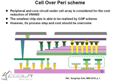
P.S. Here is a slide I found with Cell over Peri:

3245468_1474240882004.jpeg


(So a way to make the die smaller at any given capacity)
 

Glaring_Mistake

Senior member
Mar 2, 2015
310
117
116
Have you seen this yet:

170808-120053.jpg


It came from this link reporting on Samsung Keynote at FMS 2017.

Lateral shrink?

Cell over Peri?

This before proceeding to Multi-stacking.

P.S. Here is a slide I found with Cell over Peri:

3245468_1474240882004.jpeg


(So a way to make the die smaller at any given capacity)

Well, seen but not looked too closely at.

Like IntelUser2000 says Cell Over Peri should be kind of what IMFT uses and Lateral shrink to mean a reduction in litography.
Not entirely sure what Multi-stacking is though.


Controller?

Also, who made the NAND?

Well, like I said I'm keeping that secret for now but if you don't mind spoilers and can keep it to yourself I could tell you in a PM.

Thanks!

Looking at the first graph (3D TLC) it is definitely is a lot worse than the second one (sub 20 MLC NAND).

So has that made you think that even sub-20nm 2D MLC NAND can be fairly resistant to voltage drift?

Ok, then here's the surprise I had in store for you: The drive using sub-20nm 2D MLC NAND does indeed use sub-20nm 2D MLC NAND but it is three-bit MLC NAND or as it is more commonly known TLC NAND.

Unexpected?
 
  • Like
Reactions: cbn