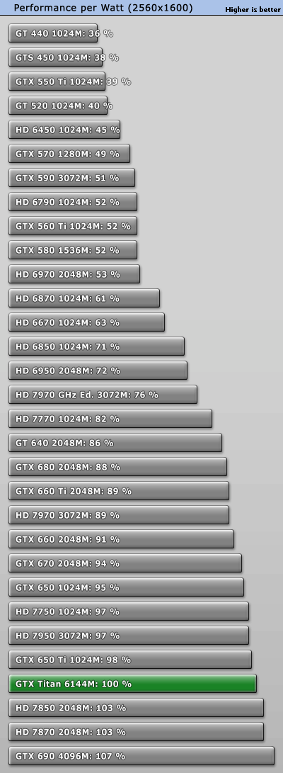
GK110 (GTX 780) 100%, 7970GHz 79%. Thats 27% better performance/watt for GK110 than Tahiti. Now think that AMD further increased core count based on same architecture. GK110 saw 55W more TDP, AMD will see how high TDP? Yeah it can`t be done with the current architecture.
Dual GPU is their only option to fight Titan or GTX 780. Spread the cores around on 2 dies and therefor spread the heat around as well. One big die can`t take this sort of heat.
You just cant talk about architecture efficiency talking about a first gen (Tahiti) die vs a second gen (GK110, its just a refined GK100 which was never released btw) die.
First of all when AMD released Tahiti the process was very immature, so Tahiti is probably engineered to work over a very leaky process, I mean it must have things like unnecesary clock routing and signaling just to guarantee a high rate of funcional dies per wafer.
There has been also a lot of discussion about the inherent inefficience caused by choosing a suboptimal ratio of the different units inside a Tahiti die. For example, there are too much shaders for only 32 ROPs, there is also a strange configuration of ROPs <--> memory channels, as the 32 ROPs cannot be mapped directly with the 6-64 bit memory channels, so theres some kind of crossbar needed between them (which adds latency, and decreases efficiency).
If you look at any review about Cape Verde, Pitcairn and Tahiti, you will see that performance scales linearly from Cape Verde to Pitcairn, but not to Tahiti (looking at shader count, Tahiti should have been around 60% faster than Pitcairn, but its only about 35%).
Look how 7870 is exactly 2x7770 (all functional units doubles and both run at 1ghz). Then you have VTX3D 7970, it runs at 1050Mhz, and its still not 60% faster than Pitcairn (despite having 60% more shaders)...
So we have about 15%/20% efficiency per watt lost only by choosing an incorrect ratio of functional units.
On top of that the 7970Ghz is only an overclocked 7970 with probably higher stock vcore to guarantee stability, that plus everything I wrote above just kills efficiency all the way, and its by no means because of the architecture.
I bet it would be very easy for AMD to release a GTX780 contender, with the same or better efficiency. The latest rumoured specs of HD8970 where 2560 shaders / 48 ROPs / 160TMUs, and I think it should fit very well into a 250watt TDP, even more, it should consume less power than the 7970GE.
Why AMD would not release this? Maybe its busy with PS4/Xbox, Kabini, Richland etc., or there's still too much stock of Tahiti based video cards, or they are just near enough to next process node and refreshing the current high-end is just a waste of resources.. I really dont know.

")