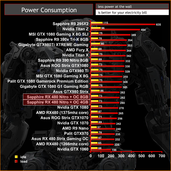
When we have pretty solid information that points to Vega being a new architecture I'm not sure why I'm reading posts bashing Polaris 10's power efficiency. Tons of people on reddit have it properly undervolted as it should have been from the start and it matches 1060 in power efficiency for the most part.
Fortunately this feature is not exclusive to Polaris 10, as you can also undervolt a GTX 1060 with good results:
http://media.bestofmicro.com/E/P/595393/original/Performance-vs.-Power-Consumption.png
>80% the stock performance at 60W.