TSMC 7nm info

Mar 10, 2006
11,715
2,012
126
From the IEDM 2016 program

A 7nm CMOS Platform Technology Featuring 4th Generation FinFET Transistors with a 0.027um2 High Density 6-T SRAM cell for Mobile SoC Applications (Late News)

So HD SRAM cell size on TSMC 7nm is 0.027um^2, roughly a 2.6x shrink from 16FF+ (0.07um^2).

Intel needs to shrink its 10nm process by a factor of 0.53x or better to maintain density leadership. But it does look like TSMC 7nm ~= Intel 10nm in terms of density.
 

happy medium

Lifer
Jun 8, 2003
14,387
480
126
GloFo's 7nm looks like it's more like TSMC's 10nm. Basically, they named it 7nm to make it look like they're on the same playing field as TSMC when they're really just posers who have yet to develop (successfully) a post-28nm node.

So Glofo is basically a second rate company making a second rate process.
 
Mar 10, 2006
11,715
2,012
126
So Glofo is basically a second rate company making a second rate process.

GloFo straight up sucks. They have been pushing power points for years about how they're going to catch up to TSMC/Intel/Samsung, but in reality they can't even take a process developed by Samsung and implement it in a satisfactory fashion.
 

happy medium

Lifer
Jun 8, 2003
14,387
480
126
TSMC/Intel/Samsung.....
Is this the current order from best to worst?
or Intel/TSMC/Samsung

How about IBM?
 
Mar 10, 2006
11,715
2,012
126
TSMC/Intel/Samsung.....
Is this the current order from best to worst?
or Intel/TSMC/Samsung

How about IBM?

Intel, TSMC, and Samsung, IMO, in terms of pure technology (though TSMC is getting really close to Intel). Other people might have different opinions though.

IBM was always good at talking up technologies that sounded good on paper, but the reality is that their technologies were always so esoteric and took forever to achieve yields acceptable for mass production (unless you are talking about IBM's own expensive, niche POWER chips that it sells as part of its systems).

Anyway, IBM was so unsuccessful as a foundry, it ended up PAYING GlobalFoundries ~$1.5B to take the fabs off of its hands.
 
  • Like
Reactions: ShintaiDK

dark zero

Platinum Member
Jun 2, 2015
2,655
138
106
Well... even HiSilicon is doing better chips than GloFo. No wonder why AMD decided to move to Samsung and let GloFo the making of the worst models in the new contract.
 
  • Like
Reactions: Glo.

witeken

Diamond Member
Dec 25, 2013
3,899
193
106
From the IEDM 2016 program

So HD SRAM cell size on TSMC 7nm is 0.027um^2, roughly a 2.6x shrink from 16FF+ (0.07um^2).

Intel needs to shrink its 10nm process by a factor of 0.53x or better to maintain density leadership. But it does look like TSMC 7nm ~= Intel 10nm in terms of density.

Woah! This is a Failure since this is their high density cell! Let me explain.

On 20 November 2015, I made a few predictions about the foundries' 10nm/7nm nodes.

  • For Intel, I predicted a 1.84x (0.54x) shrink for their high density cell from their 14nm node, which is exactly the same shrink as 22nm->14nm (I was being nicely conservative here, so as you will see I can't be accused of fanboyism; this is also based on Intel's comments that they would again shrink very aggressively at 10nm). This would result in a 0.0272µm²F (forecast) cell.
  • Since TSMC has now confirmed a cell of 0.027µm², this makes Intel's 10nm basically exactly on par with TSMC's 7nm. (For me this is no surprise given that TSMC (and Samsung) skipped a name, going from 20 to 14/16 without shrink, but this confirms that.)
  • This also confirms that Intel's 10nm, if on par, will have a great advantage on TSMC and Samsung's 10nm while they are preparing their 7nm. Intel's current SRAM density vs. TSMC is 1.4x, so this will also hold or increase at 10nm.
Now we can use this information to compare 10nm further.
  • Since Samsung's HD 10nm is 0.040µm², that puts Intel at approximately 1.47x denser (if they shrink 1.84x). TSMC will thus have a similar advantage on Samsung's 10nm, since Samsung is not planning to have fast time to market 7nm, but they will probably do a bigger shrink.
  • For TSMC 10nm, I had predicted a cell size of 0.0364µm²F (forecast, but see next bullet point) based on their statement of a 1.92x (0.52x) shrink.
  • However, I do want to stress that SRAM does not scale like the theoretical value of logic. For instance, Intel's 1.84x SRAM shrink falls short of the predicted 1.97x shrink based on transistor area (and even shorter from the real world 2.2x value), which is a delta of 7%. So if I had to make a new prediction, I would shrink TSMC's 16nm SRAM by 1.84x as well, for a TSMC 10nm SRAM size of 0.038µm²F (forecast).
  • This cell size would result in 7nm being only a 1.41x shrink, which seems a bit low. In any case, this clearly shows that TSMC's 7nm is more of a half node shrink from their 10nm, which of course is not surprising given the really short time delta between TSMC 10 and 7. But calling this a full node 7nm is bogus.
  • TSMC has claimed a 1.63x shrink of 10nm. This is of course still possible for logic. But SRAM is a really reliable number to compare a node's density, so those numbers show a lot.
So, why did I call this a failure?
  • The SRAM HD cell size that I had predicted for TSMC was based on a 1.75x shrink, which was between their reported 40-45% number. Now if I take my 10nm prediction and divide by 1.63, I get 0.023µm², which is still 15% smaller value than what TSMC now reported. My number from November 2015 was 0.0207µm². However, if you would have asked one year ago, I would have denied TSMC's 7nm would launch within 1 year of its 10nm, so I guess those 2 things sort of compensate: shorter time to market but not a big shrink.
  • But still, as Arachnotronic says, the SRAM shrink from 28nm is only 2.6x. FYI, the theoretical scaling based on node number is (28/7)² = 16x. LOL.

Finally, some speculation. I wonder why TSMC's 7nm is such a relatively small shrink. I think this could have to do with two factors. First, TSMC saw that it would lose the 10nm Apple business to Samsung. Second, TSMC saw that its 10nm would not be competitive with Intel's forecasted 10nm, which would explain the very similar SRAM size. Third, maybe some technical reason, like maybe getting everything out of DUV triple patterning before going to EUV at 5nm.


It's good news for companies that are using TSMC's 7nm tech!
Well, based on time to market I would call it decent, if you go from Samsung's 10nm to TSMC's 7nm and then to Samsung's 7nm, you might have a decent yearly improvement if you're Apple.

GloFo's 7nm looks like it's more like TSMC's 10nm. Basically, they named it 7nm to make it look like they're on the same playing field as TSMC when they're really just posers who have yet to develop (successfully) a post-28nm node.
Absolutely wrong, @Arachnotronic . GloFo's 7nm will be a real foundry 7nm node, with its fin pitch of 30nm. It should be very comparable to Intel's 10nm.

http://www.extremetech.com/computin...t-process-full-node-shrink#comment-2900604658

So Glofo is basically a second rate company making a second rate process.
They have time to market gap, sure, but they will really skip the foundry 10nm node.

GloFo straight up sucks. They have been pushing power points for years about how they're going to catch up to TSMC/Intel/Samsung, but in reality they can't even take a process developed by Samsung and implement it in a satisfactory fashion.
We'll see if the IBM purchase will result in anything. Of course I've been saying for years that there will be consolidation, so I'm not paying any serious attention to GloFo, but they do what they can with their resources... I guess :D.
 

witeken

Diamond Member
Dec 25, 2013
3,899
193
106
From the IEDM 2016 program
Wait, is there any news from Intel?

Edit: This also seems to be from TSMC?

A 7nm FinFET Technology Featuring EUV Patterning and Dual Strained High Mobility Channels (Late News)
"Dual strained" ... "High Mobility"... Haha, you won't tell me that TSMC will have III-V and Ge channels :D at 7nm. The mentioning of EUV patterning however leads me to think this is more a proof of concept than anything else. But if that is why TSMC is in such a rush to get 7nm out of the doors, then hats off to them.
 
Last edited:

ShintaiDK

Lifer
Apr 22, 2012
20,378
145
106
So...
TSMC 7nm = Intels 10nm.
Glofo 7nm = TSMC 10nm/Intels 14nm.

And then there is the electrical characteristics as well that would just make the compare even more silly.

Many names for a dear child.
 

Trumpstyle

Member
Jul 18, 2015
76
27
91
Last edited:

witeken

Diamond Member
Dec 25, 2013
3,899
193
106
So...
TSMC 7nm = Intels 10nm.
Glofo 7nm = TSMC 10nm/Intels 14nm.

And then there is the electrical characteristics as well that would just make the compare even more silly.

Many names for a dear child.
GloFo 7nm = TSMC 7nm = Intel 10nm.

With the = sign signaling equality within 10% margin of error. At the point, there is not enough information for a more precise comparison.
 
Last edited:

witeken

Diamond Member
Dec 25, 2013
3,899
193
106
It's pretty crazy, year 2018 is when TSMC officially becomes the most advanced transistor technology company in the world.

2018: Tsmc 7 nm > intels 10 nm
2020: Tsmc 5 nm > Intels 7 nm

I could not even believe Im writing this myself 2 weeks ago, but it happened. Tsmc will surpass Intel very soon.

Proof:
https://www.semiwiki.com/forum/content/6192-tsmc-16nm-10nm-7nm-5nm-update.html
With all due respect, but your post is just as much nonsense as the person of you nickname and avatar.

You, sir, are very, very lucky that I have not (yet?) published my burning analysis of your article you are claiming as proof, since you can be sure I disentangled this article completely to the bone. This article, and now I am being very polite, is full of [censored]. It is based on wrong information and the mathematics are completely wrong. You could not have written a more FUD and misleading and incorrect article.

If you would in fact have read the TS, you would have seen that your inequality sign in favor of TSMC should in fact be a shameful 7 = 10 equality sign. And as you can see, 2016 is almost over and there is no sign of TSMC 10nm. So both the numbers and dates are FUD.

The reason I sound so harsh is because I do not tolerate intellectual dishonesty. As a public site communicating about semiconductors, SemiWiki (should) have the journalistic obligation to inform people correctly instead of using this site, which people without knowledge think is a reliable site, for their TSMC agenda.

You are simply spreading lies.

Eidt: Original post referred to https://www.semiwiki.com/forum/content/6192-tsmc-16nm-10nm-7nm-5nm-update.html, but the new link isn't any better, just FYI.
 
Last edited:

ShintaiDK

Lifer
Apr 22, 2012
20,378
145
106
It's pretty crazy, year 2018 is when TSMC officially becomes the most advanced transistor technology company in the world.

2018: Tsmc 7 nm > intels 10 nm
2020: Tsmc 5 nm > Intels 7 nm

I could not even believe Im writing this myself 2 weeks ago, but it happened. Tsmc will surpass Intel very soon.

Proof:
https://www.semiwiki.com/forum/content/6160-2016-leading-edge-semiconductor-landscape.html
(edited the link(was wrong))

Semiwiki is pretty much a TSMC PR site.
 
  • Like
Reactions: witeken

carop

Member
Jul 9, 2012
91
7
71
GloFo's 7nm looks like it's more like TSMC's 10nm.

Most people appear to have missed the most important piece of information in GF's N7 technology announcement:

The process supports 17 layers of metal and could require 80-84 masks steps to handle up to quad patterning on some critical layers.

http://www.eetimes.com/document.asp?doc_id=1330467&page_number=2

You can easily infer two things from this:

First, they are moving to 1D design levels because mapping 2D design levels onto (double) spacer technology is notoriously difficult.

Second, quad patterning (SAQP) on some critical layers means that they could deliver metal pitches as small as 20nm. They will probably deliver metal pitches about 32nm in N7 technology. This would enable them to reuse most of their equipment to deliver metal pitches about 22nm in N5 technology.

The 17 layers of metal is probably for IBM POWER10.
 

witeken

Diamond Member
Dec 25, 2013
3,899
193
106
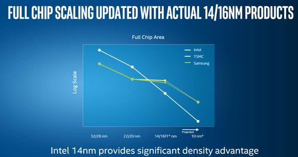
Maybe at Investor Meeting Intel will update following slide to include 7nm, although that might not yet be possible with only SRAM size known. Or probably not because then they would also have to show their own 7nm, which they won't see since it will still be 4 years out.

fullchip-intel-claim_large.png


Or maybe Bill Holt's successor will do something different completely than the usual slide deck (yield status update, density update, etc.).
 

Trumpstyle

Member
Jul 18, 2015
76
27
91
With all due respect, but your post is just as much nonsense as the person of you nickname and avatar.

You, sir, are very, very lucky that I have not (yet?) published my burning analysis of your article you are now claiming as proof, since you can be sure I disentangled your article completely to the bone. Your article, and now I am being very polite, is full of [censored]. It is based on wrong information and the mathematics are completely wrong. You could not have written a more FUD and misleading and incorrect article.

If you would in fact have read the TS, you would have seen that your inequality sign in favor of TSMC should in fact be a shameful 7 = 10 equality sign. And as you can see, 2016 is almost over and there is no sign of TSMC 10nm. So both your numbers and dates are FUD.

The reason I sound so harsh is because I do not tolerate intellectual dishonesty. As a public site communicating about semiconductors, you (should) have the journalistic obligation to inform people correctly instead of using this site, which people without knowledge think is a reliable site, for your TSMC agenda.

You are simply spreading lies.

Eidt: Original post referred to https://www.semiwiki.com/forum/content/6192-tsmc-16nm-10nm-7nm-5nm-update.html, but the new link isn't any better, just FYI.

Sorry missed your post before, seems people are just criticizing my link without explaining what is wrong with it. My understanding about transistors are not so deep but I'm open why it is wrong.

But in your post before you say Tsmc 7nm (0.027µm²) > Intel 10 nm (0.0272µm²). So even you predict Tsmc take leadership in 2018.

a
 

ShintaiDK

Lifer
Apr 22, 2012
20,378
145
106
TSMCs 10nm was to be a late 2015/2016 product too. 16FF was a 2014 product. 20nm a 2012 product.

I am sure you can see the common denominator.

You compare foundry roadmap to a product roadmap.
 
Mar 10, 2006
11,715
2,012
126
Sorry missed your post before, seems people are just criticizing my link without explaining what is wrong with it. My understanding about transistors are not so deep but I'm open why it is wrong.

But in your post before you say Tsmc 7nm (0.027µm²) > Intel 10 nm (0.0272µm²). So even you predict Tsmc take leadership in 2018.

22nm -> 14nm yielded a shrink of HDC SRAM from 0.092um^2 -> 0.0499 um^2. (scaling factor of 0.542).

Applying the same scaling factor gives 0.02707um^2 -- pretty much the same as TSMC.

Intel needs to achieve a scaling factor of 0.0541x or better to match/exceed TSMC in this metric, which is probably doable.

The point though is that Intel is feeding its investors a line of BS by saying that it's "almost a full generation ahead." This is true when we look at 10nm to 10nm comparisons, but the fact that TSMC is moving 7nm into production in early 2018 means that in terms of density Intel and TSMC are neck-and-neck (Intel's 10nm will go into production likely in late Q2/early Q3 2017 to support the Q4 2017 RTS timeline for CNL-Y).

In terms of "process superiority," Intel will need to win this one on transistor performance.
 

ShintaiDK

Lifer
Apr 22, 2012
20,378
145
106
TSMC is willing to make products when yield is ~10%. Intel likes yields to be at least 75%.
 

carop

Member
Jul 9, 2012
91
7
71
GloFo 7nm = TSMC 7nm = Intel 10nm.

With the = sign signaling equality within 10% margin of error. At the point, there is not enough information for a more precise comparison.

Is this for SRAM density, logic density, or both?

SRAM density is mainly determined by CGP (Contacted Gate Pitch) in one direction and isolation pitch in the other direction. MP (Metal Pitch) is usually not a limiting factor because an SRAM column only needs four metal lines: Vdd, Vss, BL, and BLB. (BL: Bit Line, BLB: Bit Line Bar/Complement) Furthermore, in a FinFET manufacturing technology the choice of fin pitch entangles the metal and isolation pitch together.

On the other hand, logic density to the first order is determined by CGP × MP. As such, metal and isolation pitch can be adjusted independently to meet the logic and SRAM density targets.

Curiously, neither the foundry nor the IDM has disclosed its metal pitch yet.