Question Speculation: RDNA2 + CDNA Architectures thread

Page 8 - Seeking answers? Join the AnandTech community: where nearly half-a-million members share solutions and discuss the latest tech.

uzzi38

Platinum Member
Oct 16, 2019
2,635
5,976
146
All die sizes are within 5mm^2. The poster here has been right on some things in the past afaik, and to his credit was the first to saying 505mm^2 for Navi21, which other people have backed up. Even still though, take the following with a pich of salt.

Navi21 - 505mm^2

Navi22 - 340mm^2

Navi23 - 240mm^2

Source is the following post: https://www.ptt.cc/bbs/PC_Shopping/M.1588075782.A.C1E.html
 

Glo.

Diamond Member
Apr 25, 2015
5,711
4,558
136
Any word on which 7nm process is being used? N7 EUV would certainly have helped on the efficiency front.
Absolutely nothing concrete. The only thing that is whispered to me is that "there might be clock speeds increase". My sources are hesitant to spoil anything about AMD's products, I do understand why(heck, even there is a chance that there won't be N10 refresh, and they simply will discount the current GPUs, and that is all they will do with them), but...

I guess we will know more in three weeks time.
 

DisEnchantment

Golden Member
Mar 3, 2017
1,608
5,810
136
Well ... speculation time again ... because #StayAtHome

Big Navi :cool:
Assumptions
  • 505 mm2 Dies Size
1590933345912.png
CUs
  • 4x Shader Engines
  • 2x Shader Arrays per Shader Engine
  • 5x WGPs per Shader Array
    • Increasing WGPs in the shader array can lead to lower shader occupancy like in Vega 64 so 5 WGP in a shader array is more balanced.
  • CU is 1.3x the transistor count of RDNA1
Total CU count = (4x Shader Engines) * (2x Shader Arrays per Engine) * (5x WGP per Array) * (2x CUs per WGP) = 80 CUs

Async Compute Engines
  • 8x Async Compute Engines. Each Async Compute Engine handle one shader array

Memory+Cache
  • 1x Memory Controller per Shader Array
  • 4x L2 per Memory Controller
    • In RDNA the L2 is always attached to the memory controller.
  • L2 slice size increased to 512KB, this is a configurable value from 64 to 512 KB
  • Bus Width = (4 Shader Engines) * (2 Shader Arrays per engine) * (64 Bit Memory controller) = 512Bit
  • 16 Gbps memory@512Bits = 1TB/s BW
  • (16 Gigabit GDDR6 IC) * (4 Shader Engines) * (2 Shader Arrays per engine) = 16 GB
  • Total L2 Cache = 512KB * 4 * 8 = 16MB
L2 cache is global across all Shader Engines and is used pretty much like a CPU cache, increasing it will improve hit rate and improve performance.
The increased L2 with BW increase should help with data throughput needed for RT


Alternative configuration
  • Die Size around 460mm2
  • (3x Shader Engines) * (2x Shader Arrays per Engine) * (6x WGP per Array) * (2x CUs per WGP) = 72 CUs
  • (3x Shader Engines) * (2x Shader Arrays per Engine) * (64 Bit Memory controller) =384 Bit Bus
  • 18 Gbps GDDR6 @ 384bit = 864GB/s
  • Memory = 16 Gigabit GDDR6 IC * (3 Shader Engines) * (2 Shader Arrays per engine) = 12 GB
  • L2 = 12MB
  • 6x Async Compute Engines
 

Olikan

Platinum Member
Sep 23, 2011
2,023
275
126
IMHO... RDNA2 will double (or more) the L0 cache...

Acting as a buffer since the Intersection engines need the CUs for some calculations, store the BVH instructions, and the TMUs textures...
 

DisEnchantment

Golden Member
Mar 3, 2017
1,608
5,810
136
IMHO... RDNA2 will double (or more) the L0 cache...

Acting as a buffer since the Intersection engines need the CUs for some calculations, store the BVH instructions, and the TMUs textures...
The L0 is part of the WGP/CU and indeed I have made a guesstimate for the CU above to grow in transistor count vs RDNA1.

Just plain speculation follows...

Assuming there is a small density gain of ~10-12% going from RDNA1 to RDNA2 and a 1.3x gain in area (in the previous post I meant area not transistor count)
RDNA1 CU = 84 MTr. RDNA2 CU = 84 * 1.3*1.12 = 122 MTr (45%+ gain in transistor count) [Numbers calculated using Navi10 and XSX SoC as references]

The internal cache hierarchy of the RDNA1 is very sophisticated. And we can be sure RDNA2 will improve and extend this even further even if not radically. How this transistor will be split at WGP level is anybody's guess

WGP Level cache hierachy [1x LDS per WGP and 2x L0 per WGP/1x L0 per CU]
[Some programming caveats here which could hamper performance and mentioned by Lou Kramer in her Optimization guide, due to L0 not being coherent across the WGP]
  • LDS (64K x 2)
    • Accessible by both CUs in a WGP
  • L0 (16K)
    • Accessible only from CU
    • TMU works with L0
Shader Array Level [1x L1 per shader array]
  • L1 (128K )
    • Accessible only by WGPs/CU inside the Shader Array.
Global
  • L2 (64-512K) [4x L2 slices per Shader Array]
    • Globally accessible, assumed to be doubled from 256K to 512K per slice for a total of 16MB over a 512Bit interface
    • Improving this cache and increasing the capacity as well as compression efficiency will greatly help in bandwidth efficiency.
  • GDS
    • Used for shader export to the display engine
1590951133903.png


1590951394118.png

If you compare this to Vega, you will realise how advanced RDNA is compared to GCN/Southern Islands architecture.
  • I suspect/hope the Primitive Units to be more sophisticated and enhanced to support even more culling per clock (currently 2 per clock) and stop potentially irrelevant steps from executing unnecesarily.
  • One of the things I suspect that RDNA1 performance is not scaling with memory clock is probably because it is not so much constrained by BW between L2 and the GDDR6 but between the different Shader Arrays/Engines subcomponents.
  • There is a mention of Infinity Fabric, really interested between which blocks it is being used
 

DisEnchantment

Golden Member
Mar 3, 2017
1,608
5,810
136
I checked out the branch and quickly went through the diff...

Basically using Navi10 infrastructure, so nothing new or exciting features can be gleaned from the patches yet.
Seems like a consumer chip, has no SRIOV support, in SW at least. Has no PCI ID, but internal code indicates it is GFX103X

Changes from this patch
  • New Display Core
    • DCN 2.1 --> 3.0
  • New Video Core
    • VCN 2.1 --> 3.0
    • Lots of new encoders/decoder blocks
    • Supports JPEG 3.0
  • Minor SMU Update
    • 11.0 --> 11.0.7
  • Exposed new PCI Audio device
    • 0x1002, 0xab28
Seems like there are two new clock domains for the Video and Display engine, so 2 clock domains for Display and 2 clock domains for Video.
Major takeaway is that there are major changes in the display and video subsystem which should be good. (I read a bunch of patents lately for AMD and most of their patents are related to power efficiency in Video transcoding and compression. Could be related here)
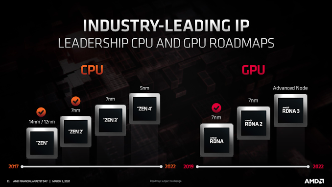
Last major jump was from Vega to Navi10.

One tidbit that I found is that in emulation mode, they are using only 128bit GDDR6. I don't know what it means, it could be that the chip is a small mobile variant or possibly this is of no meaning and only used for emulation.
It is still intriguing because the value is fetched from the atomfirmare which is probably not available in emulation mode and they just hard coded it.
C++:
    if (adev->asic_type == CHIP_SIENNA_CICHLID && amdgpu_emu_mode == 1) {
        adev->gmc.vram_type = AMDGPU_VRAM_TYPE_GDDR6;
        adev->gmc.vram_width = 1 * 128; /* numchan * chansize */
    } else {

UPDATE:
This whole naming and misleading comments and branches is simply some obfuscation in the code.
I think when everything will be squared up they will do clean up.
 
Last edited:

DisEnchantment

Golden Member
Mar 3, 2017
1,608
5,810
136
That slide is not AMD, the quotes are european ones :D, but I agree to the dual VCN 3.0 instances, I found that in the code too.
There are dual clock domains for VCN.
Also this is a dGPU and features deep sleep and ultra low voltage operation.
Still very unsure what this Dual Pipe Graphics command processor.

There is indeed a newer SDMA v5.2. I need to look up the instances and the PP table tomorrow.
 
  • Like
Reactions: Tlh97 and bearmoo
Mar 11, 2004
23,075
5,557
146
Rampant speculation about the VCN:
1.) Maybe they use video encoding block to apply DLSS type of image processing?
2.) They put two in for game streaming, where there's some input (i.e. camera) and this way one would be for the combined output while the other dedicated for processing the direct game footage that you'd see on a display?
3.) Return of All-in-Wonder capabilities with video input. Could be used for a variety of things (game streaming from external, maybe video editing).
4.) Its for Eyefinity type of scenarios where it can be used for multiple displays/feeds (juggling that for video processing/editing, viewing a need for that after Apple's Afterburnerer card) with a bunch of displays (think video walls and other stuff).
3.) Could they also possibly use video overlay processing for certain effects? Like reflections? Or managing HUD/GUI stuff separately?
4.) VR per eye? Or some other VR targeted aspect (i.e. doing a pixel shifting type of affect that could provide perceived resolution boost while not actually having to render it).
5.) Staged, where one could handle lower resolutions or lower framerates and is optimized for power efficiency, while another is there for higher resolutions and/or framerates.
 

DisEnchantment

Golden Member
Mar 3, 2017
1,608
5,810
136
XGMI support for Cichlid can be found in the source code. Also there certifications of XGMI bridges online by RRA and FCC.
Also the Atombios firmware has entries to read out if the chip is being liquid cooled.
Additionally, there is support added for I2C access to the Infineon VRM which can deliver upto 500-1000A of current at 1.3V
This is certainly not Arcturus because it uses the GFX10.3 and GMC10 blocks.
There is a beast hidden behind these seemingly benign and docile comments with misleading code paths and omitted sections.
Interesting times ahead.
 

GodisanAtheist

Diamond Member
Nov 16, 2006
6,817
7,177
136
Looks like September is when we'll know more:


Computex is scheduled for late September, so figure it'll happen then if we're not in lockdown phase 2.
 

Krteq

Senior member
May 22, 2015
991
671
136
Some new "Sienna Cichlid" related commits in RadeonSI MESA driver

Some interesting stuff there:

ac_gpu_info.c
Code:
if (info->chip_class >= GFX10_3)
        info->max_wave64_per_simd = 16;
    else if (info->chip_class == GFX10)
        info->max_wave64_per_simd = 20;
    else if (info->family >= CHIP_POLARIS10 && info->family <= CHIP_VEGAM)
        info->max_wave64_per_simd = 8;
From RDNA whitepaper:
The fetched instructions are deposited into wavefront controllers. Each SIMD has a separate instruction pointer and a 20-entry wavefront controller, for a total of 80 wavefronts per dual compute unit. Wavefronts can be from a different work-group or kernel, although the dual compute unit maintains 32 work-groups simultaneously. The new wavefront controllers can operate in wave32 or wave64 mode.
So, according to that commit, in Sienna there is 16-entry wavefront controller per SIMD
 
  • Like
Reactions: Olikan

kurosaki

Senior member
Feb 7, 2019
258
250
86
How about this one? Debunked or could it be in the right ballpark. Look at those RAM-figures...
182279_O.png
 

DisEnchantment

Golden Member
Mar 3, 2017
1,608
5,810
136
Were GDDR6X confirmed by Jedec or some manufacturer yet?
JEDEC a global leader in developing open standards has done a good job hiding them?
For over 50 years, JEDEC has been the global leader in developing open standards and publications for the microelectronics industry. JEDEC committees provide industry leadership in developing standards for a broad range of technologies.
 

Stuka87

Diamond Member
Dec 10, 2010
6,240
2,559
136
JEDEC a global leader in developing open standards has done a good job hiding them?

Well first, they have never "hid" standards before. And it kind of goes against everything a standard is. The whole purpose of being a standard is that it has to go through a ratification process. When GDDR5X or GDDR6 came out, we knew well ahead of time what they were and when they were going to go into production.