@PeterScott I have to agree with you on this as making "Super" APU for PC would be a costly item to make with a limited niche. I'm also thinking that most folks who need more then 4c/8t will want a video card instead of a limited iGPU anyway.

Speculation: AMD's APU with HBM
Page 2 - Seeking answers? Join the AnandTech community: where nearly half-a-million members share solutions and discuss the latest tech.
You are using an out of date browser. It may not display this or other websites correctly.
You should upgrade or use an alternative browser.
You should upgrade or use an alternative browser.
frozentundra123456
Lifer
- Aug 11, 2008
- 10,451
- 642
- 126
Bingo. That was my point actually. The OP left out the most obvious response of whether it will ever happen at all. We have been hearing speculation for years from the AMD camp about this killer APU. I thought the pointless speculation had finally died, but I guess not.Maybe never?
In fact it has been quite the opposite. AMD has seemed to push the majority of their resources into Ryzen chips without an igpu at all. They are still stuck on 4 cores for APUs.
Last edited:
William Gaatjes
Lifer
- May 11, 2008
- 19,550
- 1,193
- 126
If it is not HBM2, it is probably not worth it.
https://www.anandtech.com/show/9969/jedec-publishes-hbm2-specification
The cpu normally has two 64 bit controllers. HBM2 supports that 64 bit channel mode and legacy HBM not.
I guess it depends on how the memory controller and cache controller works, how many bytes are retreived at once when the cpu wants to access memory that is not in the cache. And how many bytes are written.
I doubt AMD could even spare the money or the manpower to developed such a product with a very limited niche market anyway. For that matter why would they want to?Bingo. That was my point actually. The OP left out the most obvious response of whether it will ever happen at all. We have been hearing speculation for years from the AMD camp about this killer APU. I thought the pointless speculation had finally died, but I guess not.
In fact it has been quite the opposite. AMD has seemed to push the majority of their resources into Ryzen chips without an igpu at all. They are still stuck on 4 cores for APUs.
I for one wither have a separate video card and CPU due to being more likely to need to upgrade the GPU then both the dGPU and CPU at the time. And beside I think that a 8c/16t CPU will last me for years.
LightningZ71
Golden Member
- Mar 10, 2017
- 1,627
- 1,898
- 136
But that's the whole point of products like KadyG. You use it to save the cost of a full discrete you setup in a laptop. There is a considerable market for laptops in the less than $1000 price range with mid-range gpus that can push decent frame rates at 1080p and maybe a bit above. Kady G can already do that to an extent. A possible 3400g/h, which is speculated to be the 12 nm refresh for Raven ridge, would be the natural choice for the CPU die, an 8x PCIe gen 4 interface would work for the pgpu link, and there would be a space for a hbm stack or two as well.
The advantage here is that the Apu can be used in it's various target markets without the mcm/interposer, or with the interposer/mcm, and the same package can be used with a higher end CPU that doesn't have an iGPU for higher end products or for the sff/aio/stb/console market. It gives maximum market flexibility with maximum investment reuse. And, since most of the configuration changes are in the processor package, the only changes that the notebook manufacturers will need to make are for cooling or I/O layout needs.
This is far from niche and has broad applicability in many different segments. My personal opinion on why KadyG isn't making better market penetration are two fold. First is cost. It appears that Intel wants a lot of money for this product. That is the result of their segmentation strategy pushing KadyG's price north of their already expensive Iris Pro products. The other issue is the decision to make the "Vega" GPU for KadyG a Polaris product with a HBM interface with the thermal issues included. Add in the high cost of HBM and it's going to be hard for vendors to make margin initially.
PeterScott
Platinum Member
- Jul 7, 2017
- 2,605
- 1,540
- 136
But that's the whole point of products like KadyG. You use it to save the cost of a full discrete you setup in a laptop. There is a considerable market for laptops in the less than $1000 price range with mid-range gpus that can push decent frame rates at 1080p and maybe a bit above. Kady G can already do that to an extent. A possible 3400g/h, which is speculated to be the 12 nm refresh for Raven ridge, would be the natural choice for the CPU die, an 8x PCIe gen 4 interface would work for the pgpu link, and there would be a space for a hbm stack or two as well.
The advantage here is that the Apu can be used in it's various target markets without the mcm/interposer, or with the interposer/mcm, and the same package can be used with a higher end CPU that doesn't have an iGPU for higher end products or for the sff/aio/stb/console market. It gives maximum market flexibility with maximum investment reuse. And, since most of the configuration changes are in the processor package, the only changes that the notebook manufacturers will need to make are for cooling or I/O layout needs.
This is far from niche and has broad applicability in many different segments. My personal opinion on why KadyG isn't making better market penetration are two fold. First is cost. It appears that Intel wants a lot of money for this product. That is the result of their segmentation strategy pushing KadyG's price north of their already expensive Iris Pro products. The other issue is the decision to make the "Vega" GPU for KadyG a Polaris product with a HBM interface with the thermal issues included. Add in the high cost of HBM and it's going to be hard for vendors to make margin initially.
It's KabyLake G. Not Kady anything.
Really there is no cost advantage for Kaby-G, and it isn't an APU.
An actual APU, that is small in size, with normal memory requirements is a good and cost effective product.
Kaby-G is just a discrete CPU and a discrete GPU coexisting on a small PCB, saving nothing in buying them separately.
I will have price the Kaby-G but isn't a mid-range dGPU and CPU cheaper to buy then this is?It's KabyLake G. Not Kady anything.
Really there is no cost advantage for Kaby-G, and it isn't an APU.
An actual APU, that is small in size, with normal memory requirements is a good and cost effective product.
Kaby-G is just a discrete CPU and a discrete GPU coexisting on a small PCB, saving nothing in buying them separately.
Has there been a decision whether MCM packages can be considered an "APU"? For starters I think "APU" is more a brand thing... but I haven't made up my mind about the MCM vs single die thing because it's not really come up until now.It's KabyLake G. Not Kady anything.
Really there is no cost advantage for Kaby-G, and it isn't an APU.
An actual APU, that is small in size, with normal memory requirements is a good and cost effective product.
Kaby-G is just a discrete CPU and a discrete GPU coexisting on a small PCB, saving nothing in buying them separately.
And I'd argue there are direct cost savings with a MCM solution from simplicity of motherboard design, if not simply from logistical a perspective. Though this obviously has to be balanced with increased cost from complexity of the MCM.
cbn
Lifer
- Mar 27, 2009
- 12,968
- 221
- 106
Compared to a CPU + dGPU on one package (like Kabylake-G)....an APU (either monolithic die or die to die via Infinity fabric):
1.) Can shift the entire TDP to either CPU or iGPU.
Think about how nice it would be do Blender purely on the iGPU (with the full TDP available) while having high bandwidth access to system memory (rather than having to go over PCIe bus like a dGPU would).
Likewise imagine being able to get the full TDP budget to the CPU for OpenShot. (or the full TDP budget to the iGPU for Hit Film Video editor*)
*Unlike OpenShot which uses the CPU only for rendering, Hit Film does the opposite and uses only the GPU for rendering.
2.) Allows the system DDR4 and HBM to be used by either CPU or iGPU in a high bandwidth fashion**. (So in a system with 8GB DDR4 and 4GB HBM the CPU or iGPU each has access to 12GB memory).
**Kabylake-G's dGPU only has access to the DDR4 system RAM over PCIe bus (which is much lower bandwidth than an APU using Infinity fabric to connect GPU to CPU)
Last edited:
Both of these assume IF is much faster than PCIe, but I haven't seen much info comparing them in reality. I know IF is scalable, but so is PCIe up to a certain point.Compared to a CPU + dGPU on one package (like Kabylake-G)....an APU (either monolithic die or MCM via Infinity fabric):
1.) Can shift the entire TDP to either CPU or iGPU.
Think about how nice it would be do Blender purely on the iGPU (with the full TDP available) while having high bandwidth access to system memory (rather than having to go over PCIe bus like a dGPU would).
Likewise imagine being able to get the full TDP budget to the CPU for OpenShot. (or the full TDP budget to the iGPU for Hit Film Video editor*)
*Unlike OpenShot which uses the CPU only for rendering, Hit Films does the opposite and uses only the GPU for rendering.
2.) Allows the system DDR4 and HBM to be used by either CPU or iGPU in a high bandwidth fashion**. (So in a system with 8GB DDR4 and 4GB HBM the CPU or iGPU each has access to 12GB memory).
**Kabylake-G's dGPU only has access to the DDR4 system RAM over PCIe bus (which is much lower bandwidth than an APU using Infinity fabric to connect GPU to CPU)
I think of IF as an AMD in-house and more versatile version of PCIe, which can work over the exact same pins as PCIe. For example I understand my Ryzen + Vega system is technically capable of using IF to connect the two over the PCIe x 16 hardware. IIRC the IF connection would be slightly faster than PCIe v3, but it wouldn't be heaps faster simply because it's IF vs PCIe like you're implying. So is the internal IF in an APU wider or clocked higher? And will this always be the case?
PeterScott
Platinum Member
- Jul 7, 2017
- 2,605
- 1,540
- 136
Has there been a decision whether MCM packages can be considered an "APU"? For starters I think "APU" is more a brand thing... but I haven't made up my mind about the MCM vs single die thing because it's not really come up until now.
If you consider Kaby-G an APU, then it is basically a useless term that doesn't differentiate anything significant.
We always had discrete parts, the whole point of the APU was fusing those into a single die:
https://www.amd.com/en-us/press-releases/Pages/amd-fusion-apu-era-2011jan04.aspx#
"The AMD Fusion Family of Accelerated Processing Units (APUs) incorporate - in a single die design - multi-core CPU (x86) technology, a powerful DirectX®11-capable discrete-level graphics and parallel processing engine, a dedicated high-definition video acceleration block, and a high-speed bus that speeds data across the differing types of processor cores within the design."
That was the whole point for an APU, for cost and production efficiency. I single die to do the whole duty for the most expensive computer parts. Simplified design and low cost parts. This vision was a driver for the merger of AMD and ATI.
And I'd argue there are direct cost savings with a MCM solution from simplicity of motherboard design, if not simply from logistical a perspective. Though this obviously has to be balanced with increased cost from complexity of the MCM.
It's a wash IMO. You don't have to connect the CPU to GPU using the main motherboard because you are using a tiny motherboard to connect them and to the main motherboard. That really isn't likely any kind of cost savings outside of pennies. Some more traces on the Motherboard are of insignificant cost.
The big savings are true APUs like Raven Ridge. A single $99 part can power a PC or laptop for most people, with a simple square contact cooler design
The Super APU like in the Xbox is a niche that will likely never see application in PCs, and Kaby-G type designs really aren't APUs, and don't have the cost savings of a real APU.
cbn
Lifer
- Mar 27, 2009
- 12,968
- 221
- 106
Intel are struggling to penetrate the market with kaby lake G
So you think Kaby Lake-G will fail as a product?
I've read great reviews of Ultrabooks based on it, e.g. this PCWorld review.
"Today though, there are few takers of Kaby Lake G. In fact, only two vendors have shipped it: HP with the Spectre x360 15, and Dell with its XPS 15 2-in-1. Some we’ve spoken to have painted that as a failure of Kaby Lake G to catch on, while others have speculated politics to be the cause. Whatever the truth, it’s a shame, because applied the right way in the right laptop, Kaby Lake G is a road worth taking."
Interesting, it does allow power sharing (like an APU):
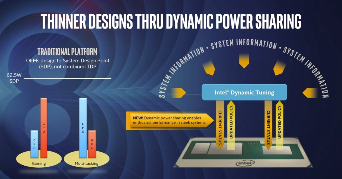
With Kaby Lake G, the power and thermal needs of the CPU, GPU, and the RAM for the GPU are all managed as one. If the module’s under a heavy graphics load, the CPU can back off. If the CPU is under a heavy load, the GPU can back off. That initially led many to assume that Kaby Lake G was paired with a lower power 15-watt “U” series chip. Kaby Lake G is instead based on an “H” part, which is rated at 45 watts and can run at 56 watts until it heats up.
That is a very good thing to see....and an advantage over a Intel CPU and Nvidia dGPU.
PeterScott
Platinum Member
- Jul 7, 2017
- 2,605
- 1,540
- 136
Both of these assume IF is much faster than PCIe, but I haven't seen much info comparing them in reality. I know IF is scalable, but so is PCIe up to a certain point.
I think of IF as an AMD in-house and more versatile version of PCIe, which can work over the exact same pins as PCIe. For example I understand my Ryzen + Vega system is technically capable of using IF to connect the two over the PCIe x 16 hardware. IIRC the IF connection would be slightly faster than PCIe v3, but it wouldn't be heaps faster simply because it's IF vs PCIe like you're implying. So is the internal IF in an APU wider or clocked higher? And will this always be the case?
IIRC off die IF uses re-purposed PCIe lanes, so it is just PCIe running a different protocol.
Yes that's what I understand also. And this is how Epyc works in a multi CPU setting, and even how the intercommunication between the chiplets in each "CPU" work. Same for MCM IF in Threadripper which also uses "re-purposed PCIe lanes", but I assume it's similar (if not identical) to the IF in Raven Ridge (where we can't use the term "re-purposed PCIe lanes").IIRC off die IF uses re-purposed PCIe lanes, so it is just PCIe running a different protocol.
So I don't see any physical difference between "re-purposed PCIe lanes" and "IF lanes", thus I'm not sure what you're trying to say.
I'm genuinely interested how single die IF is different to MCM IF and how they both compare with "external" IF over PCIe lanes. Because I've seen a lot of claims here that IF is in a different league to PCIe but I've seen very little hard facts...
Last edited:
IntelUser2000
Elite Member
- Oct 14, 2003
- 8,686
- 3,785
- 136
Kaby-G is just a discrete CPU and a discrete GPU coexisting on a small PCB, saving nothing in buying them separately.
Kabylake-G isn't a "discrete CPU and discrete GPU on a small PCB". No, its on a single package, which is the first step in integration.
Aimed at the right segment, it can save costs due to lower components on the PC board. In this case though, I'm assuming the higher thermal density requirements and not being able to reuse board design contribute to costs being a wash. Cost to consumer can't be explained by a single reason.
Theoretically, Kabylake-G can deliver smaller form factors/better battery life/better perf watt/lower cost. Of course you can't choose them all. Likely though the realistic aim is same, or even slightly higher cost, but go into smaller form factors at similar performance and offer better battery life. Intel knows thinner/lighter gaming devices can be priced higher.
Interesting, it does allow power sharing (like an APU):
Power sharing has so far been used improve performance/watt by lowering power, not by improving performance. Kabylake-G is the first attempt at doing the latter.
I think cases where games show significant deficiency compared to average happen because it needs more firmware and driver optimization. Of course, it won't win at everything.
Last edited:
NTMBK
Lifer
- Nov 14, 2011
- 10,237
- 5,019
- 136
A part with low-cost HBM on the package substrate could make sense for laptops- we already saw Intel doing something very similar with EDRAM. If AMD want to keep their integrated graphics faster than Intel, they're going to need something similar- DDR4 bandwidth isn't going to cut it for much longer. Even Raven Ridge is already heavily bottlenecked.
cbn
Lifer
- Mar 27, 2009
- 12,968
- 221
- 106
Where is the option for "It will be a long time, if ever, before we see a consumer APU with HBM"?
Maybe never?
Since Kaby G is out, I wouldn't say that.
But if you want to put it into categories, lets see.
1) AMD APU with HBM
2) APU with HBM that's common, like Raven Ridge
#1 is probably likely in the near future, but similar to Kaby G it should remain high end. #2 is far less likely. Separate memory stacks will always cost more. The problem in the value space is always that extra packaging adds cost, even if the memory stack is very cheap.
I agree #1 is likely. (It would be a high end part).
Also if AMD uses the 8C/16T CPU die (as part of a BGA APU) it could potentially have the full 32 PCIe 3.0 lanes (not 24 PCIe 3.0 lanes as seen in socket AM4).
That would be really nice for a workstation level laptop (Thinking about how a person could have various combinations of NVMe NAND*, Optane and Thunderbolt III controllers. This in addition to two SATA 6 Gbps ports native to the CPU die.)
*RAID-0 would be interesting for certain types of data driven work. (With the Optane being used for the small files)
- Oct 22, 2004
- 799
- 1,351
- 136
If it is not HBM2, it is probably not worth it.
In this speculation thread, I have used HBM as a generic term for High Bandwidth Memory, with no regard to the specific version, or generation, of the particular HBM specification.
If you consider Kaby-G an APU, then it is basically a useless term that doesn't differentiate anything significant.
In this discussion, since we are speculating about the future, I think we need to see the APU chip as a black box, and accept any form of integration within that black box, including MCM solutions.
MCM solutions based on new packaging technology and "chiplet" design is an inevitable part of the roadmap of the industry, it seems, as monolithic die design hits its limits.
MCM solutions based on new packaging technology and "chiplet" design is an inevitable part of the roadmap of the industry, it seems, as monolithic die design hits its limits.
the whole point of the APU was fusing those into a single die
Well, that's merely what Intel did.
As a programmer by profession, I view HSA as the overarching vision for AMD's Fusion design philosophy — in particular, the simplification of the programming model and memory model of the system, with seamless and coherent memory access, reduced latency, pre-emptive task switching, and a standardised API and hardware-agnostic ISA for the heterogeneous compute units in the system.
As a programmer I face two kinds of algorithms; sequential and parallel. Some of the latter runs very well on a GPU, but to this day, I have never taken advantage of that, even though my 20+ years old software (road design) may be very well suited for that and see massive speed and efficiency gains.
Why? It is not easy. There are some tools (such as C++ AMP) that are promising, and the C++ language standard committee is now doing great work to enable parallelisation seamlessly. But there is still a long way to go before running computations on a GPU is as simple as running them on the CPU.
For example, a game should seamlessly be able to use all hardware acceleration available on a system. Even if a discrete GPU card is present and runs the game's main graphics load, the game should take advantage of the gigaflops of parallel compute performance available in todays integrated GPUs. Just disabling such a powerful coprocessor is a sad waste. In the future, maybe a game will use the integrated GPU to run AI, while using the discrete GPU for the graphics load.
To bring my digression back on topic; my interest in APUs are not for graphics, and not to replace more powerful discrete cards for gamers and professional users that need them. I am interested in technology, and I'd like to see HSA become reality, so that programmers can simply and seamlessly make use of any acceleration available in their user's systems. A big part of that is to remove bottlenecks in memory latency and bandwidth — which is what this discussion is about.
Last edited:
- Oct 22, 2004
- 799
- 1,351
- 136
My personal opinion on why [Kaby Lake-G] isn't making better market penetration are two fold. First is cost. It appears that Intel wants a lot of money for this product.
And contributing to that, it is likely that AMD charges a pretty sum for the GPU as well, to ensure the chip doesn't directly compete with its own mainstream APU products. On top of that, the EMIB packaging technology is cutting-edge. And HBM2 is relatively expensive.
Adoption may also be limited due to production capacity, in particular packaging. Intel may have decided to do a limited roll-out for this reason, only so far partnering with HP and Dell on two models. There is also the plausible hypothesis that Apple wants this solution and require substantial volume dedicated to their plans.
My thinking is that Intel had a brief window of opportunity for this product. They figured out what was coming on AMD's roadmap — that an APU with HBM would be inevitable — and saw the opportunity to respond before AMD was ready with their own all-AMD solution. I respect the agility and pragmatism shown by Intel in this. But they had to rush it, while pioneering a completely new, and hence costly, packaging solution.
If AMD doesn't come out with their own all-AMD solution at 7nm (2019-2020), I will be very surprised.
It seems that one of the arguments being used to say that APU means a single piece of silicon is the following.
Using two die on a interposer is the same as using the traditional means of connecting GPU and CPU, namely PCIe lanes. This is misleading, but quite tempting as an argument.
Two main benefits of an interposer versus the traditional are :
1) The # of connections possible. Rivaling internal SOC connections in quantity. This is NOT possible with traditional wires on a PCB.
2) The added latency of a signal is ~1ns for the interposer connection. [Given in a Xilinx paper].
With regards to cost efficiency, it will always be cheaper to fab two smaller die than a single larger one of close to equal size of the sum. The reintegration costs are the decider and those are dropping continually with volume increases and new methods.
The ability to more easily bin for more valuable properties [power, speed] and to choose the best foundry process for each sub-unit is another property that an integrated, one die SOC will never have.
PeterScott
Platinum Member
- Jul 7, 2017
- 2,605
- 1,540
- 136
Kabylake-G isn't a "discrete CPU and discrete GPU on a small PCB". No, its on a single package, which is the first step in integration.
You are just mincing words.
The "single package" is a small PCB. EMIB is only used between HBM and the discrete GPU, while standard PCB interconnects and PCIe is used between the discrete CPU and discrete GPU.
- Oct 22, 2004
- 799
- 1,351
- 136
You are just mincing words.
Less arguing and more speculating, please.
")
IntelUser2000
Elite Member
- Oct 14, 2003
- 8,686
- 3,785
- 136
My thinking is that Intel had a brief window of opportunity for this product.
There's a PCWatch article about this.
It was that they wanted HBM for client, but they did not have parts with HBM compatible memory controllers. eDRAM was just a temporary solution until they had the proper CPU.
Supposedly it would have been around the Icelake generation, as it was in the days when it was expected 10nm would go along without a hitch. Without the 10nm(and 14nm) delay, the Icelake chips would have been scheduled for mid 2017.
Last edited:
PeterScott
Platinum Member
- Jul 7, 2017
- 2,605
- 1,540
- 136
Less arguing and more speculating, please.
We still need accuracy even when speculating.
TRENDING THREADS
-
 Discussion Intel current and future Lakes & Rapids thread
- Started by TheF34RChannel
- Replies: 23K
-
 Discussion Zen 5 Speculation (EPYC Turin and Strix Point/Granite Ridge - Ryzen 9000)
- Started by DisEnchantment
- Replies: 10K
-
Discussion Intel Meteor, Arrow, Lunar & Panther Lakes Discussion Threads
- Started by Tigerick
- Replies: 7K
-

-

AnandTech is part of Future plc, an international media group and leading digital publisher. Visit our corporate site.
© Future Publishing Limited Quay House, The Ambury, Bath BA1 1UA. All rights reserved. England and Wales company registration number 2008885.