[Rumour] TSMC will produce the huge GP100 interposer

raghu78

Diamond Member
Aug 23, 2012
4,093
1,475
136
http://www.bitsandchips.it/52-english-news/6816-rumor-tsmc-will-produce-the-huge-gp100-interposer

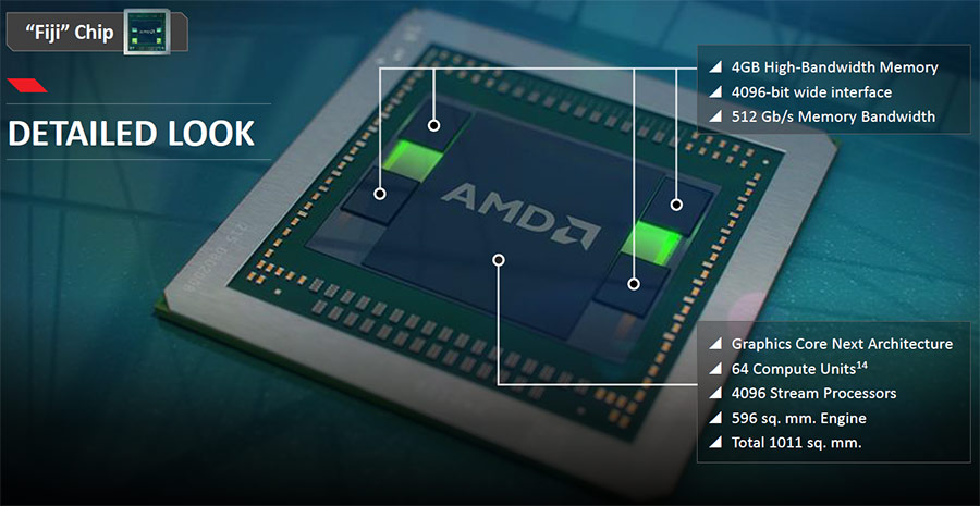
"According to our source, TSMC is sampling the Interposer for the next GP100 NVIDIA GPUs … and it will be huge! We talking about a 1200 mm2 interposer (Fiji interposer is about 1000 mm2)."

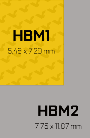
So will Nvidia and TSMC be able to get such a complex big die GPU on a massive interposer right the first time around. Nvidia has no experience with HBM2 and 2.5D stacking. TSMC has experience as they have developed FPGAs with Xilinx which utilize interposers.

http://www.ispd.cc/slides/2013/0_madden.pdf

The interposer size is even bigger than Fiji's. Well Nvidia seems to be going all out with GP100 to defend its HPC turf from Intel Knights Landing. :D
 

ShintaiDK

Lifer
Apr 22, 2012
20,378
145
106
Sounds like a bigtime pile of BS. No wonder with the source.

Fiji interposer is even outside the limit. Aka no metal layers outside the area. Adding 200mm2 more without any metal layers...I dont think so.

Finally, as large as the Fiji GPU is, the silicon interposer it sits on is even larger. The interposer measures 1011mm2, nearly twice the size of Fiji. Since Fiji and its HBM stacks need to fit on top of it, the interposer must be very large to do its job, and in the process it pushes its own limits. The actual interposer die is believed to exceed the reticle limit of the 65nm process AMD is using to have it built, and as a result the interposer is carefully constructed so that only the areas that need connectivity receive metal layers. This allows AMD to put down such a large interposer without actually needing a fab capable of reaching such a large reticle limit.
 

Glo.

Diamond Member
Apr 25, 2015
5,711
4,556
136
He also said, in another forum, that the TSMC has some problems with production of interposer.
 

EightySix Four

Diamond Member
Jul 17, 2004
5,121
49
91
HBM2 is physically larger than HBM1 isn't it? Even if GP100 was the same size as the Fiji die it would need a larger imposer due to the size of the memory.
 

ShintaiDK

Lifer
Apr 22, 2012
20,378
145
106
HBM2 is physically larger than HBM1 isn't it? Even if GP100 was the same size as the Fiji die it would need a larger imposer due to the size of the memory.

Yes. And that's not possible. Assuming 4 stacks. I would guess the limit lies between 450 and 500mm2 GPU with 4 stacks of HBM2. With 2 stacks you can get 600mm2 again.

hbm2-vs-hbm1-size-comparison.png


And it will only keep growing in size to increase density.
 

Piroko

Senior member
Jan 10, 2013
905
79
91
HBM2 is physically larger than HBM1 isn't it? Even if GP100 was the same size as the Fiji die it would need a larger imposer due to the size of the memory.
It's not that much larger since you only need to expand the interposer in one direction. 1200mm² actually sounds about right for a 550~600mm² chip with four stacks of HBM2.

edit: See this image, there's a lot of wasted space with HBM1:
fiji-chip.jpg
 
Last edited:

Timmah!

Golden Member
Jul 24, 2010
1,419
631
136
Yes. And that's not possible. Assuming 4 stacks. I would guess the limit lies between 450 and 500mm2 GPU with 4 stacks of HBM2. With 2 stacks you can get 600mm2 again.

hbm2-vs-hbm1-size-comparison.png


And it will only keep growing in size to increase density.

I dont know about this, but it would not surprise me, if the GP100 would be just 450 mm chip. IIRC i saw somewhere a sheet saying top Pascal chip is about to give 4 TFlops of DP performance, while Volta is going to improve this number to 7. Assuming this was true, and assuming both Pascal and Volta are going to be 16nm, does that mean that 550mm- 600mm Volta chip is going to be 1,75x more powerful than 550mm - 600mm Pascal chip? Somehow i dont think so.
 

Azix

Golden Member
Apr 18, 2014
1,438
67
91
I'm actually not understanding if this is against or for the idea. Are they saying 1200mm^2 at 7nm for the future but that size is possible on another process now? or it will be only possible later?

Also, it definitely states "silicon interposers larger than 1,200mm2"

This does not exclude interposers of 1200mm^2. In fact it could suggest this is their current upper limit and has been done.

TSMC will enable silicon interposers larger than 1,200mm2 — 1.5x the reticle size — at 7nm to enable giant 2.5-D stacks of logic and memory for the next generation of what it calls Cowos (chip on wafer on substrate). The foundry taped out last month a 16FF+ device merging a CPU and two HBM2 memory stacks on a silicon interposer to pave the way for its 7nm offering.

http://www.eetimes.com/document.asp?doc_id=1329217&page_number=2
 

krumme

Diamond Member
Oct 9, 2009
5,952
1,585
136
Boom.

This bits 'n chips guy seems to be pulling crap out of thin air that even the most cursory of sanity checks would prove to be false.
Read the stuff and pls stop the selective quoting (phynaz). For some reason Fottemberg needs to be attacked and i guess its about the usual fan war right? Childish behavior for rumors about a imposer.

" The foundry taped out last month a 16FF+ device merging a CPU and two HBM2 memory stacks on a silicon interposer to pave the way for its 7nm offering."
 

itsmydamnation

Platinum Member
Feb 6, 2011
2,772
3,148
136
Yes. And that's not possible. Assuming 4 stacks. I would guess the limit lies between 450 and 500mm2 GPU with 4 stacks of HBM2. With 2 stacks you can get 600mm2 again.

hbm2-vs-hbm1-size-comparison.png


And it will only keep growing in size to increase density.

Where are the bumps Shintai?
 

Doom2pro

Senior member
Apr 2, 2016
587
619
106
I'm pretty sure the Interposer size limitations are due to the reticle limits...

Unless they radically change the production process it will stay at that limit.
 

Azix

Golden Member
Apr 18, 2014
1,438
67
91
I'm pretty sure the Interposer size limitations are due to the reticle limits...

Unless they radically change the production process it will stay at that limit.

its suggested the interposer is not limited by this. I think fiji interposer already exceeds the limit. Quick google search shows some patents and articles suggesting interposers exceeding the reticle limit.
 
Feb 19, 2009
10,457
10
76
It's inconceivable for a 450mm2 Pascal chip to meet the FP64 performance metrics that they have touted.

Intel's KL is a solid challenger and Pascal will be the same huge monolithic chip to rise to that challenge, IMO.
 

JDG1980

Golden Member
Jul 18, 2013
1,663
570
136
Fiji interposer is even outside the limit. Aka no metal layers outside the area. Adding 200mm2 more without any metal layers...I dont think so.

Here is what TechReport says about Fiji's interposer, based on an interview with Raja Koduri:

The reason why Fiji isn't any larger, he said, is that AMD was up against a size limitation: the interposer that sits beneath the GPU and the DRAM stacks is fabricated just like a chip, and as a result, the interposer can only be as large as the reticle used in the photolithography process. (Larger interposers might be possible with multiple exposures, but they'd likely not be cost-effective.)

Note the bolded part. What's not cost-effective on a sub-$1000 video card might well be viable on a HPC card costing ten times as much.
 

Pottuvoi

Senior member
Apr 16, 2012
416
2
81
It's inconceivable for a 450mm2 Pascal chip to meet the FP64 performance metrics that they have touted.

Intel's KL is a solid challenger and Pascal will be the same huge monolithic chip to rise to that challenge, IMO.
Whats the current rumor on FP64 performance?
Isn't the data movement/power usage the biggest problem, not the die space for FP units?
 

itsmydamnation

Platinum Member
Feb 6, 2011
2,772
3,148
136
All over the package. What you expect, packed into a corner?

Really got anything to back that up? because i cant find any. They most certainly could be be on one side, there is a logic die that sits at the bottom of the stack. Chipworks dont have any free images showing the logic die layer connecting to the interposer All the pics i have seen have the phy on the logic die on the edge closest to the main die.

You also realise that fiji has an imposer size around 800mm sq as fiji die size is just under 600 sq mm.


edit: look at page 10 here:
http://www.hotchips.org/wp-content/...Bandwidth-Kim-Hynix-Hot Chips HBM 2014 v7.pdf
 
Last edited:

ShintaiDK

Lifer
Apr 22, 2012
20,378
145
106
You also realise that fiji has an imposer size around 800mm sq as fiji die size is just under 600 sq mm.

1011mm2 isn't 800mm2.

Finally, as large as the Fiji GPU is, the silicon interposer it sits on is even larger. The interposer measures 1011mm2, nearly twice the size of Fiji. Since Fiji and its HBM stacks need to fit on top of it, the interposer must be very large to do its job, and in the process it pushes its own limits. The actual interposer die is believed to exceed the reticle limit of the 65nm process AMD is using to have it built, and as a result the interposer is carefully constructed so that only the areas that need connectivity receive metal layers. This allows AMD to put down such a large interposer without actually needing a fab capable of reaching such a large reticle limit.
 

itsmydamnation

Platinum Member
Feb 6, 2011
2,772
3,148
136
1011mm2 isn't 800mm2.

yes a took an eyeball guess, 600mm + 35mm X 4 + some extra. But you just confirmed my point for me. From an interposer perspective you can have a dark side of the dram stack. So for GP100 it only has to have part of the Dram stack on the part of the interposer that can route wires.

The question then becomes one of bump density and complexity/number of metal layers in the base die as to how much of a DRAM stack needs to be routeable (for lack of a better word).
 

antihelten

Golden Member
Feb 2, 2012
1,764
274
126
Really got anything to back that up? because i cant find any. They most certainly could be be on one side, there is a logic die that sits at the bottom of the stack. Chipworks dont have any free images showing the logic die layer connecting to the interposer All the pics i have seen have the phy on the logic die on the edge closest to the main die.

You also realise that fiji has an imposer size around 800mm sq as fiji die size is just under 600 sq mm.


edit: look at page 10 here:
http://www.hotchips.org/wp-content/...Bandwidth-Kim-Hynix-Hot Chips HBM 2014 v7.pdf

The microbumps are placed in a rectangle in the middle of the HBM1 die and consists of 53 columns and 104 rows (not all spots are populated though, so there are only 4942 bumps total instead of 5512).

As such the microbumps are indeed spread all over the package as Shintai said, with the exception of the edge of the die (there's a border region of 0.5-1 mm with no bumps)

You find the layout of the microbumps on HBM1 here (the coordinates are in µm). I couldn't find a link for HBM2 unfortunately

Edit: Just noticed, but the presentation you linked actually has a picture of the microbump layout on slide 13. I attached a cropped image:
5OozHjr.jpg


Yep, in other words. The technology isn't even there yet.

Actually, it probably is. Phynaz link dealt with interposers larger than 1200mm2, which doesn't really have anything to do with the topic at hand (a 1200mm interposer).

TSMC has been making functional interposers up to 1200mm2 (1248mm2 to be exact) since at least 2013, so it wouldn't be terribly surprising if they managed to get it production ready by now.
 
Last edited: