Rumored specifications for HD8850/8870 - Launch January 2013 (?)

RussianSensation

Elite Member
Sep 5, 2003
19,458
765
126
HD8850 - 28nm Oland Pro

3.4 billion transistors
~ 270mm-280mm^2 die
925mhz GPU clock (975mhz Boost)
1536 Shaders
96 TMUs (93.6 GTexels/sec texture fill-rate)
32 ROPs (31.2 GPixels/sec pixel fill-rate)
6 Ghz GDDR5 @ 256-bit (192 Gb/sec memory bandwidth)
TDP 130W
(Single-Precision Compute: 2.99 Tflops, 187 Gflops Double Prec.)
Comparable performance to GTX670, 35% faster than GTX 660 2.0GB

HD8870 - 28nm Oland XT

3.4 billion transistors
~ 270mm-280mm^2 die
1050mhz GPU clock (1100mhz Boost)
1792 Shaders
112 TMUs (123.2 GTexels/sec texture fill-rate)
32 ROPs (35.2 GPixels/sec pixel fill-rate)
6 Ghz GDDR5 @ 256-bit (192 Gb/sec memory bandwidth)
TDP 160W
(Single-Precision Compute: 3.94 Tflops, 246 Gflops Double Prec.)
Comparable performance to GTX680, 30% faster than GTX 660Ti 2.0GB

Also rumored to have some "AMD Wireless Display Technology" (?)

Launch: January 2013?

*** Take with a huge grain of salt due to random source***

http://read2ch.com/r/jisaku/1347605134/ID:hKcZJDn

>>> Personally I think this sounds way too good to be true since we are still stuck at 28nm (unless 28nm node has matured this much behind the scenes). If true, we are looking at GTX680 level of GPU performance next year at $349 I bet.
 
Last edited:
Feb 19, 2009
10,457
10
76
Beefed up 7870 core, with its high power efficiency. Not at all unsurprising given a 7950 with similar specs at those clock speed is already ~= 680.

What's suprising is the really fast refresh, a new die and not just higher clocks.

Edit: RS, you shouldn't be all that suprised.. you can already get 680 perf for ~$300 with 7950 and a mild OC.

What im looking forward to is GK110 and how beastly it will be.
 
Last edited:

AnandThenMan

Diamond Member
Nov 11, 2004
3,949
504
126
Interesting. I don't think these specs are out of the realm of possibility, with layout and process improvements it actually looks about right to me.

Can we extrapolate from this what a 8950/8970 might be all about?
 
Feb 19, 2009
10,457
10
76
Can we extrapolate from this what a 8950/8970 might be all about?

Nope, because we have nothing concrete on the die size. I'm not expecting major perf/mm2 improvements (clock for clock), so perf should correlate with die size and clock speed increases only.
 

RussianSensation

Elite Member
Sep 5, 2003
19,458
765
126
Edit: RS, you shouldn't be all that suprised.. you can already get 680 perf for ~$300 with 7950 and a mild OC.

:biggrin:

Took 6-7 months for NV to match HD7950/7870 with GTX660Ti/660 in performance and it looks like it will take less than 6 months from today for HD8850/8870 will deliver 20-25%+ performance increase over NV's mid-range parts. Good times ahead.

I suppose they can get away with 160-175W TDP on those parts since Oland doesn't have the double precision compute of Tahiti. Makes sense that they enlarged Pitcairn further and started working off its already efficient layout.

I wonder how they will deal with a larger die size / power consumption for HD8950/8970 parts if they keep full DP capabilities of Tahiti XT?
 

LOL_Wut_Axel

Diamond Member
Mar 26, 2011
4,310
8
81
Some of those specs just look wrong. For example, the die size. There's no way the HD 8800 series will have a die that is 270-280mm^2, especially with a 256-bit bus. It needs to be in either a similar or lower power envelope than the HD 7800 series. There's no way you're gonna get that with a die that's 60-70mm^2 bigger on the same process technology. If the die is bigger, it's gonna be 20-30mm^2 bigger at most.

The memory speed looks off as well. AMD has always made the memory speed different between the two cards of a series. 5.0-5.5GHz GDDR5 sounds right for the HD 7850, and 6GHz sounds right for the HD 7870.

Anyway, we'll see. January-March 2013 looks to be about the right timeframe to release the series.
 

RussianSensation

Elite Member
Sep 5, 2003
19,458
765
126
HD8800 series is a lean gaming chip, just like HD7800 series is. Why can't you fit 256-bit bus into a 280mm^2 die when NV fit it into a 294mm^2 die? You are looking at a 27-32% increase in die size (270-280) from Pitcairn XT.

By that point the 28nm node will have had 12 months of manufacturing maturity. I think they can get a 280mm^2 die chip @ 160-170W with 1100mhz GPU clocks.
 

LOL_Wut_Axel

Diamond Member
Mar 26, 2011
4,310
8
81
HD8800 series is a lean gaming chip, just like HD7800 series is. Why can't you fit 256-bit bus into a 280mm^2 die when NV fit it into a 294mm^2 die? You are looking at a 27-32% increase in die size (270-280) from Pitcairn XT.

By that point the 28nm node will have had 12 months of manufacturing maturity. I think they can get a 280mm^2 die chip @ 160-170W with 1100mhz GPU clocks.

It would be very easy to fit a 256-bit bus into a 280mm^2 die. The problem is, it wouldn't make any sense given they already have a product with a 256-bit bus in a 212mm^2 die with Pitcairn.

Let's take a small look back at history:
Cypress (HD 5800 series) measured 334mm^2.
Power consumption for HD 5870 averaged 143 watts in games.

Cayman (HD 6900 series) measured 389mm^2.
Power consumption for HD 6970 averaged 202 watts in games.

They're not 100% comparable because of VLIW4 vs. VLIW5, but you get the point. If the die is any significant amount bigger, power consumption will go up.
 

AnandThenMan

Diamond Member
Nov 11, 2004
3,949
504
126
40nm@TSMC was really terrible, I don't think you can make a good comparison based on it. My prediction is that much greater improvements will be realized on 28nm.
 

toyota

Lifer
Apr 15, 2001
12,957
1
0
well cant the chip be way more efficient? GK110 certainly delivered more performance with less power consumption. the GTX580 was 15-20% faster than the GTX480 while using less power.
 

LOL_Wut_Axel

Diamond Member
Mar 26, 2011
4,310
8
81
well cant the chip be way more efficient? GK110 certainly delivered more performance with less power consumption. the GTX580 was 15-20% faster while using less power.

Not comparable because the GF100 was terribly optimized. They made some optimizations, and performance/watt increased by 30-40% in GF110.

AMD has worked out how to make things as efficient as possible from the get go for a long time now.
 

LOL_Wut_Axel

Diamond Member
Mar 26, 2011
4,310
8
81
40nm@TSMC was really terrible, I don't think you can make a good comparison based on it. My prediction is that much greater improvements will be realized on 28nm.

Right...

The HD 5870 consumes on average ~145W in games. The HD 7970 consumes on average ~190W in games.
 

toyota

Lifer
Apr 15, 2001
12,957
1
0
Not comparable because the GF100 was terribly optimized. They made some optimizations, and performance/watt increased by 30-40% in GF110.

AMD has worked out how to make things as efficient as possible from the get go for a long time now.
it is comparable because hardly anyone thought that would even be possible...
 

LOL_Wut_Axel

Diamond Member
Mar 26, 2011
4,310
8
81
So essentially you are saying is that on 28nm, AMD will not be able to realize any efficiency improvements? Ridiculous.

They will, but nowhere near as big as is being said here. Like in the past: significantly bigger die=higher power consumption.

Nice try at twisting my words, though.
 

LOL_Wut_Axel

Diamond Member
Mar 26, 2011
4,310
8
81
it is comparable because hardly anyone thought that would even be possible...

No, it is not.

GF100 was rushed to the market. Pitcairn was not.

Examples of GF100 being unoptimized for low power consumption:

As a result NVIDIA had to look at GF110 at a transistor level, and determine what they could do to cut power consumption. Semiconductors are a near-perfect power-to-heat conversion device, so a lot of work goes in to getting as much work done with as little power as necessary. This is compounded by the fact that dynamic power (which does useful work) only represents some of the power used – the rest of the power is wasted as leakage power. In the case of a high-end GPU NVIDIA doesn’t necessarily want to reduce dynamic power usage and have it impact performance, instead they want to go after leakage power. This in turn is compounded by the fact that leaky transistors and high clocks are strange bedfellows, making it difficult to separate the two. The result is that leaky transistors are high-clocking transistors, and vice versa.

Thus the trick to making a good GPU is to use leaky transistors where you must, and use slower transistors elsewhere. This is exactly what NVIDIA did for GF100, where they primarily used 2 types of transistors differentiated in this manner. At a functional unit level we’re not sure which units used what, but it’s a good bet that most devices operating on the shader clock used the leakier transistors, while devices attached to the base clock could use the slower transistors. Of course GF100 ended up being power hungry – and by extension we assume leaky anyhow – so that design didn’t necessarily work out well for NVIDIA.


For GF110, NVIDIA included a 3rd type of transistor, which they describe as having “properties between the two previous ones”. Or in other words, NVIDIA began using a transistor that was leakier than a slow transistor, but not as leaky as the leakiest transistors in GF100. Again we don’t know which types of transistors were used where, but in using all 3 types NVIDIA ultimately was able to lower power consumption without needing to slow any parts of the chip down. In fact this is where virtually all of NVIDIA’s power savings come from, as NVIDIA only outright removed few if any transistors considering that GF110 retains all of GF100’s functionality.
http://www.anandtech.com/show/4008/nvidias-geforce-gtx-580/3
 
Last edited:

tviceman

Diamond Member
Mar 25, 2008
6,734
514
126
www.facebook.com
HD8850 - 28nm Oland Pro

3.4 billion transistors
~ 270mm-280mm^2 die
925mhz GPU clock (975mhz Boost)
1536 Shaders
96 TMUs (93.6 GTexels/sec texture fill-rate)
32 ROPs (31.2 GPixels/sec pixel fill-rate)
6 Ghz GDDR5 @ 256-bit (192 Gb/sec memory bandwidth)
TDP 130W
(Single-Precision Compute: 2.99 Tflops, 187 Gflops Double Prec.)
Comparable performance to GTX670, 35% faster than GTX 660 2.0GB

HD8870 - 28nm Oland XT

3.4 billion transistors
~ 270mm-280mm^2 die
1050mhz GPU clock (1100mhz Boost)
1792 Shaders
112 TMUs (123.2 GTexels/sec texture fill-rate)
32 ROPs (35.2 GPixels/sec pixel fill-rate)
6 Ghz GDDR5 @ 256-bit (192 Gb/sec memory bandwidth)
TDP 160W
(Single-Precision Compute: 3.94 Tflops, 246 Gflops Double Prec.)
Comparable performance to GTX680, 30% faster than GTX 660Ti 2.0GB

Also rumored to have some "AMD Wireless Display Technology" (?)

Launch: January 2013?

*** Take with a huge grain of salt due to random source***

http://read2ch.com/r/jisaku/1347605134/ID:hKcZJDn

>>> Personally I think this sounds way too good to be true since we are still stuck at 28nm (unless 28nm node has matured this much behind the scenes). If true, we are looking at GTX680 level of GPU performance next year at $349 I bet.

If the specs are true, then Oland will likely have the same memory bandwidth performance issues that plague Kepler (or worse, since Nvidia usually manages to squeeze better performance out of the same or less mem bandwidth as AMD cards in each comparable generation).

Anyways, performance sounds pretty close to what I would guess (perhaps a little optimistic, I think a stock hd8780 will be about 10% slower than a stock gtx680), but that sounds like a pretty big die for a second tier AMD GPU.
 

ocre

Golden Member
Dec 26, 2008
1,594
7
81
:biggrin:

Took 6-7 months for NV to match HD7950/7870 with GTX660Ti/660 in performance and it looks like it will take less than 6 months from today for HD8850/8870 will deliver 20-25%+ performance increase over NV's mid-range parts. Good times ahead.
...........

anyone else dizzy from from all the spinning yet? Just spewing out non-stop bull till eventually it starts to stick.

How can anyone take this serious? None of it makes good sense, its much more correct to say:
took AMD 14months to get up to 580 performance with Tahiti. A couple more months on top the 14 to almost get to 580 levels with the 7870. AMD finally matched their own 6970 performance. With the 7700 AMD managed to match the power of GPUs literally from several years ago. and i can go one and on annoyingly spouting utter crap to try to paint things in the boldest negative colors possible. ;yawn
pretty lame.

But seriously, Nvidia finally matched the power of the 7800 series yet they had cards that could bet them out for many many months. Nvidia finally matched 7800 series performance when the 7800 series launched offering zero performance increase per dollar of cards from past generations. they came out and wasnt a better value, they also didnt perform any better than what was already on the market..... over a year ago. I mean, no one finally matched the performance of the 7800series cause that performance had been around for a long while before they ever hit the street.

This is really ridiculous and pretty pointless to debate. its kinda funny to see people try so hard all the time. I mean, why do you always have to say stuff like this? its a statement that is so forced into the topic it dont belong at all. The rest of the post doesnt go with it. Why is there consistent jabs all the time? Consistently placed and sloppy attempts for what reasons? I mean AMD is cool and all but why the constant forced in nvidia jabs?

So i guess what i am saying is the first part of the post is complete utter nonsense that makes me want to say.........chill, we know you dont like nvidia get over it already.

The 2nd part, well this
I suppose they can get away with 160-175W TDP on those parts since Oland doesn't have the double precision compute of Tahiti. Makes sense that they enlarged Pitcairn further and started working off its already efficient layout.

I wonder how they will deal with a larger die size / power consumption for HD8950/8970 parts if they keep full DP capabilities of Tahiti XT?

I wonder this too. What are they gonna do? What can they do?

Pitcain is really efficient and imagine if they could do something very BIG with it. It would make a killer gaming GPU if they built up. Sort of like the gk104 but perhaps even more redesigning. could you imagine building it up to 200watts? This could be an interesting direction. But its just me dreaming

i dont even know if we should take any of these early rumors serious, i mean not yet. I also dont expect the 8000 series till much later than January, but thats just my thinking. I dont know what or how it will be but it has me thinking a lot. The possibilities.........
 

LOL_Wut_Axel

Diamond Member
Mar 26, 2011
4,310
8
81
You said, "as efficient as possible from the get go" those are your words.

Yes. And...?

That doesn't account for things like better yields and lower leakage, both of which come naturally as the process node matures. You're not gonna get anywhere near the improvement this article is saying when you've already made your current product as efficient as you can with what you have available.

The situation with NVIDIA and GF100 was simply a case of them rushing a product to market and not doing things like selecting transistors for low power consumption/low performance and high power consumption/high leakage as best as they could. If they did this, yields wouldn't have been as atrocious as they were and they would've had lower power consumption. Of course, the fact that this was their first product on the 40nm node didn't help at all. AMD had the HD 4770 to test.
 

toyota

Lifer
Apr 15, 2001
12,957
1
0
No, it is not.

GF100 was rushed to the market. Pitcairn was not.

Examples of GF100 being unoptimized for low power consumption:

http://www.anandtech.com/show/4008/nvidias-geforce-gtx-580/3
I am not denying that GF100 was not unoptimized. the POINT is that nobody thought we would get a full version of the gpu that was not only faster but used less more power. heck a GTX590 looked like an impossible dream there for a while.

so would you need to do is open your mind and realize that it is possible for things to happen that may not seem 100% possible to you.
 

LOL_Wut_Axel

Diamond Member
Mar 26, 2011
4,310
8
81
]I am not denying that GF100 was not unoptimized. the POINT is that nobody thought we would get a full version of the card that was not only faster but used less more power.[/B] heck a GTX590 looked like an impossible dream there for a while.

so would you need to do is open your mind and realize that it is possible for things to happen that may not seem 100% possible to you.

It makes a lot of sense when you read the article and explanation, actually. Again, GF100 was rushed to market/unoptimized and Pitcairn was not. Simple as that.
 

BallaTheFeared

Diamond Member
Nov 15, 2010
8,115
0
71
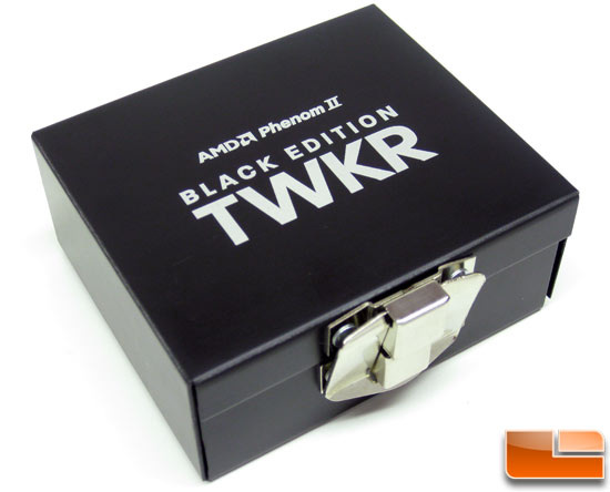
Leaky transistors can be a good thing, with proper cooling.

AMD's TWKR's are an example of that practice.

amd_twkr_cpu_case.jpg
 

sze5003

Lifer
Aug 18, 2012
14,182
625
126
Should I wait for the 8870 or not..January seems far to go without a card at all :(
 

AnandThenMan

Diamond Member
Nov 11, 2004
3,949
504
126
Yes. And...?

That doesn't account for things like better yields and lower leakage, both of which come naturally as the process node matures. You're not gonna get anywhere near the improvement this article is saying when you've already made your current product as efficient as you can with what you have available.
You just contradicted yourself. What AMD had available when they were designing SI is not what they have available now.