Polaris 10 and 11 confirmed to be GDDR5 based

raghu78

Diamond Member
Aug 23, 2012
4,093
1,475
136
We finally are seeing more information which finally confirms Polaris 10 and 11 are GDDR5 based.

Polaris 10 - Ellesmere
Polaris 11 - Baffin

http://www.phoronix.com/scan.php?page=news_item&px=AMD-Open-Sourced-Polaris

"The initial Baffin PCI IDs include 0x67E0, 0x67E1, 0x67E8, 0x67E9, 0x7EB, and 0x7FF. The Ellesmere IDs are 0x67C0 and 0x67DF."

"Polaris includes the ELLESMERE and BAFFIN chip families."

http://ranker.sisoftware.net/show_r...e0d2e3d4e7d0e8cebc81b197f297aa9abccff2ca&l=en

Polaris 10 - Ellesmere

36-40CU, 2304-2560 sp, 256 bit GDDR5 @ 6Ghz , 8GB.

Here is the article talking about Polaris open source code

https://lists.freedesktop.org/archives/dri-devel/2016-March/103402.html?utm_source=anzwix

We also know from earlier zauba leaks that Baffin is 4GB GDDR5.

http://wccftech.com/amd-radeon-r9-400-gpus/

We don't know if the Polaris 10 SKU seen at sisoftware is a fully enabled SKU. Anyway we can now put to rest the claims that Polaris might use HBM. The fact that Polaris 10 and 11 are GDDR5 based bodes good for pricing and availability. The other big gain is memory capacity. HBM1 was limited to 4GB and that was a problem imo. Now Polaris 10 is 8GB with 256 bit GDDR5 just as PS4. :)

My guess (based only on available info which might change)
Polaris 11 - Baffin - 1024sp, 16CU(2 x 8CU), 128 bit GDDR5, 4GB
Polaris 10 - Ellesmere - 2304-2560, 36-40CU (4 x 9 or 4 x 10 CU), 256 bit GDDR5, 192 GB/s, 8GB.
 
Last edited:

happy medium

Lifer
Jun 8, 2003
14,387
480
126
So Baffin = ~ r9 380
Ellesmere = ~ Fury/Fury X

Memory bandwidth can't be right. 192Gb/s?

Good info.
 

Head1985

Golden Member
Jul 8, 2014
1,864
688
136
390x still have 20% more SP and 512Bit vs 256bit 6Ghz.
2808 vs 2304.It will be miracle if polaris 10 match even 390x.
 

Mahigan

Senior member
Aug 22, 2015
573
0
0
Baffin is the bigger of the two Polaris GPUs. If the bigger GPU is Polaris 10 then Baffin is Polaris 10.

Baffin is an Island more than twice the size of Ellesmere Island. Greenland is evidently larger than both.

I think that we will see many SKUs and a BaffinXT would be the performance part. I'm still banking on BaffinXT using 4GB of HBM. I think that smaller Baffin SKUs may use 8GB of GDDR5.

Ellesmere will no doubt use GDDR5
 

railven

Diamond Member
Mar 25, 2010
6,604
561
126
Really wonder if it's HBM that is neutering Fiji. Considering all the specs, Fiji can't seem to escape Hawaii/Grenada with enough distance to justify the cost.
 

MrTeal

Diamond Member
Dec 7, 2003
3,569
1,698
136
Baffin is the bigger of the two Polaris GPUs. If the bigger GPU is Polaris 10 then Baffin is Polaris 10.

Baffin is an Island more than twice the size of Ellesmere Island. Greenland is evidently larger than both.

I think that we will see many SKUs and a BaffinXT would be the performance part. I'm still banking on BaffinXT using 4GB of HBM. I think that smaller Baffin SKUs may use 8GB of GDDR5.

Ellesmere will no doubt use GDDR5

What are you basing that on, other than just the physical sizes of the islands? Cape Verde is 5x larger than Tonga, so that's hardly a good rationale. The updated driver makes it pretty clear that Baffin is the smaller Polaris 11.
 

raghu78

Diamond Member
Aug 23, 2012
4,093
1,475
136
Umm, a mistake?

Because Baffin Island is larger than Ellesmere Island. I'm a canuck so I know these things. https://en.m.wikipedia.org/wiki/List_of_Canadian_islands_by_area

You are assuming that the island size have to correspond to the GPU size which need not be the case.

Baffin is the bigger of the two Polaris GPUs. If the bigger GPU is Polaris 10 then Baffin is Polaris 10.

Baffin is an Island more than twice the size of Ellesmere Island. Greenland is evidently larger than both.

I think that we will see many SKUs and a BaffinXT would be the performance part. I'm still banking on BaffinXT using 4GB of HBM. I think that smaller Baffin SKUs may use 8GB of GDDR5.

Ellesmere will no doubt use GDDR5

Here is a quote from AMD dev

https://www.phoronix.com/forums/for...code-for-next-gen-polaris?p=860390#post860390

"@Michael We're calling them Polaris 10 (was Ellesmere) and Polaris 11 (was Baffin) now, any chance you could tweak the article accordingly ?

Thanks !"

What are you basing that on, other than just the physical sizes of the islands? Cape Verde is 5x larger than Tonga, so that's hardly a good rationale. The updated driver makes it pretty clear that Baffin is the smaller Polaris 11.

correct. We also have the wccftech zauba listing showing Baffin XT as 4GB GDDR5. Now that we know Ellesmere is 8GB GDDR5 there is no more confusion. Polaris 10 - Ellesmere and Polaris 11 - Baffin.
 
Last edited:

Headfoot

Diamond Member
Feb 28, 2008
4,444
641
126
Processing unit count between architectures is not meaningful. Maxwell had less than Kepler yet crushed it. There are lots of low hanging IPC fruit in GPUs because many times it makes more sense to build out more units than to make individual units faster. But nVidia took the other route with Maxwell and perhaps AMD is too. What matters is end performance, not paper specs.

That's not even accounting for the fact that you can count processor numbers differently based on what you're counting
 

happy medium

Lifer
Jun 8, 2003
14,387
480
126
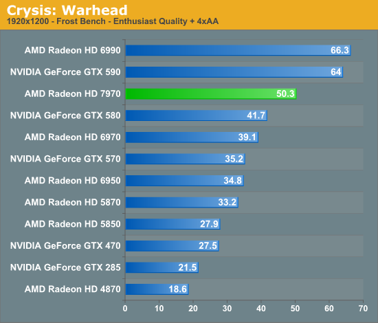
6970 40nm with 1536 sp's vs the 7970 28nm with 2048 sp's, the 7970 was ~ 20 % faster with~ 25% more sp's.

43095.png


Now we have a 28nm 390x with 2816 sp's vs a Polaris 10 @ 14nm with 2304 sp's.
How would one expect a Polaris 10 to = a 390x?

Heres what I'm thinking. Polaris 11 replaces 270x, Polaris 10 replaces 280x, and theres another Polaris 9? that replaces a 390x.

I cant find the site but I remember some site saying that there was a 3rd chip.
 
Last edited:

raghu78

Diamond Member
Aug 23, 2012
4,093
1,475
136
390x still have 20% more SP and 512Bit vs 256bit 6Ghz.
2808 vs 2304.It will be miracle if polaris 10 match even 390x.

The architecture has changed significantly and it would be wrong to assume the Polaris sp perf and efficiency is similar to earlier GCN versions.

http://venturebeat.com/2016/01/15/a...-to-full-graphics-immersion-with-16k-screens/

"We have two versions of these FinFET GPUs. Both are extremely power efficient. This is Polaris 10 and that’s Polaris 11. In terms of what we’ve done at the high level, it’s our most revolutionary jump in performance so far. We’ve redesigned many blocks in our cores. We’ve redesigned the main processor, a new geometry processor, a completely new fourth-generation Graphics Core Next with a very high increase in performance. We have new multimedia cores, a new display engine. This is very early silicon, by the way. We have much more performance optimization to do in the coming months."
 

happy medium

Lifer
Jun 8, 2003
14,387
480
126
The architecture has changed significantly and it would be wrong to assume the Polaris sp perf and efficiency is similar to earlier GCN versions.

http://venturebeat.com/2016/01/15/a...-to-full-graphics-immersion-with-16k-screens/

"We have two versions of these FinFET GPUs. Both are extremely power efficient. This is Polaris 10 and that’s Polaris 11. In terms of what we’ve done at the high level, it’s our most revolutionary jump in performance so far. We’ve redesigned many blocks in our cores. We’ve redesigned the main processor, a new geometry processor, a completely new fourth-generation Graphics Core Next with a very high increase in performance. We have new multimedia cores, a new display engine. This is very early silicon, by the way. We have much more performance optimization to do in the coming months."

Well that's eye opening , thanks for the link.
 

Mahigan

Senior member
Aug 22, 2015
573
0
0
What are you basing that on, other than just the physical sizes of the islands? Cape Verde is 5x larger than Tonga, so that's hardly a good rationale. The updated driver makes it pretty clear that Baffin is the smaller Polaris 11.

Cape Verde and Tonga didn't release at the same time.
 

raghu78

Diamond Member
Aug 23, 2012
4,093
1,475
136
6970 40nm with 1536 sp's vs the 7970 28nm with 2048 sp's, the 7970 was ~ 20 % faster with~ 25% more sp's.

43095.png


Now we have a 28nm 390x with 2816 sp's vs a Polaris 10 @ 14nm with 2304 sp's.
How would one expect a Polaris 10 to = a 390x?

Heres what I'm thinking. Polaris 11 replaces 270x, Polaris 10 replaces 280x, and theres another Polaris 9 that replaces a 390x.

I cant find the site but I remember some site saying that there was a 3rd chip.

GCN/VLIW performance comparison at launch might have been underwhelming but that changed rapidly as GCN drivers matured and game engines started targetting GCN for optimization as the consoles were all GCN based. btw Raja Koduri has confirmed there are only 2 Polaris chips in 2016 - Polaris 10 and Polaris 11. Polaris 10 is the bigger GPU and likely to replace AMD's Fury X and Fury GPUs. Polaris 11 is the smaller GPU likely to replace R9 380 and R9 380X.

btw Maxwell GTX 980 with 2048 cc easily beat Kepler GTX 780 Ti with 2880cc. So do not compare performance between 2 different architecture generations based on core count.
 

Despoiler

Golden Member
Nov 10, 2007
1,966
770
136
Really wonder if it's HBM that is neutering Fiji. Considering all the specs, Fiji can't seem to escape Hawaii/Grenada with enough distance to justify the cost.

HBM2 does add in some nice tweaks. Namely it uses pseudo channels. We've seen in one of the review that the effective bandwidth in HBM is not as close as it should be compared to it's theoretical max.

One of the key enhancements of HBM2 is its Pseudo Channel mode, which divides a channel into two individual sub-channels of 64 bit I/O each, providing 128-bit prefetch per memory read and write access for each one. Pseudo channels operate at the same clock-rate, they share row and column command bus as well as CK and CKE inputs. However, they have separated banks, they decode and execute commands individually. SK Hynix says that the Pseudo Channel mode optimizes memory accesses and lowers latency, which results in higher effective bandwidth.

http://www.anandtech.com/show/9969/jedec-publishes-hbm2-specification

That being said, FIJI does actually stretch it's legs when you feed it proper DX12 implementations. Fiji is full tilt built for DX12 using copious amounts of async compute. It suffers from low overall utilization in DX11 or what I will call DX12-lite implementations.
 

raghu78

Diamond Member
Aug 23, 2012
4,093
1,475
136
Cape Verde and Tonga didn't release at the same time.

The point he was trying to convey is the island size does not correlate to the GPU size which you are completely missing. btw there is enough information now to say that Ellesmere is Polaris 10 and Baffin is Polaris 11. Just read the information already posted in my earlier comments.
 

MrTeal

Diamond Member
Dec 7, 2003
3,569
1,698
136
I'm really not expecting a massive jump in per shader performance. Look at it this way, they demoed P11 vs a 950, a card with similar performance to 1280shader@1GHz, 212mm² Pitcairn. All indications are that P11 will be in the 100-120mm² range, which if P11 was also 1280 shaders (but clocked much lower in the test) would be a reasonable 2x scaling in density. If P10 does come in at 232mm², 2304-2560 shaders makes a lot of sense. If its shaders also perform as well at 800MHz at Hawaii at 1GHz, it might just be a hair below Hawaii in current D11 games.
 

happy medium

Lifer
Jun 8, 2003
14,387
480
126
btw Maxwell GTX 980 with 2048 cc easily beat Kepler GTX 780 Ti with 2880cc. So do not compare performance between 2 different architecture generations based on core count.

I understand what your saying but weren't the 6970 and 7970 different architectures and the 7970 was also on a different node also?

The 7970 had more cores and more performance.

I guess AMD did something special this round ha?
 

MrTeal

Diamond Member
Dec 7, 2003
3,569
1,698
136
Cape Verde and Tonga didn't release at the same time.

Then sub in Tahiti, which is a quarter the size of Cape Verde.

Code:
@@ -681,8 +681,8 @@ static uint32_t fw_type_convert(void *cgs_device, uint32_t fw_type)
 		result = AMDGPU_UCODE_ID_CP_MEC1;
 		break;
 	case CGS_UCODE_ID_CP_MEC_JT2:
-		if (adev->asic_type == CHIP_TONGA || adev->asic_type == CHIP_BAFFIN
-		  || adev->asic_type == CHIP_ELLESMERE)
+		if (adev->asic_type == CHIP_TONGA || adev->asic_type == CHIP_POLARIS11
+		  || adev->asic_type == CHIP_POLARIS10)
 			result = AMDGPU_UCODE_ID_CP_MEC2;
 		else
 			result = AMDGPU_UCODE_ID_CP_MEC1;
@@ -742,17 +742,17 @@ static int amdgpu_cgs_get_firmware_info(void *cgs_device,
 		case CHIP_FIJI:
 			strcpy(fw_name, "amdgpu/fiji_smc.bin");
 			break;
-		case CHIP_BAFFIN:
+		case CHIP_POLARIS11:
 			if (type == CGS_UCODE_ID_SMU)
-				strcpy(fw_name, "amdgpu/baffin_smc.bin");
+				strcpy(fw_name, "amdgpu/polaris11_smc.bin");
 			else if (type == CGS_UCODE_ID_SMU_SK)
-				strcpy(fw_name, "amdgpu/baffin_smc_sk.bin");
+				strcpy(fw_name, "amdgpu/polaris11_smc_sk.bin");
 			break;
-		case CHIP_ELLESMERE:
+		case CHIP_POLARIS10:
 			if (type == CGS_UCODE_ID_SMU)
-				strcpy(fw_name, "amdgpu/ellesmere_smc.bin");
+				strcpy(fw_name, "amdgpu/polaris10_smc.bin");
 			else if (type == CGS_UCODE_ID_SMU_SK)
-				strcpy(fw_name, "amdgpu/ellesmere_smc_sk.bin");
+				strcpy(fw_name, "amdgpu/polaris10_smc_sk.bin");
 			break;
 		default:
 			DRM_ERROR("SMC firmware not supported\n");


also
Code:
@@ -281,6 +281,16 @@ static struct pci_device_id pciidlist[] = {
 	{0x1002, 0x9877, PCI_ANY_ID, PCI_ANY_ID, 0, 0, CHIP_CARRIZO|AMD_IS_APU},
 	/* stoney */
 	{0x1002, 0x98E4, PCI_ANY_ID, PCI_ANY_ID, 0, 0, CHIP_STONEY|AMD_IS_APU},
+	/* Baffin */
+	{0x1002, 0x67E0, PCI_ANY_ID, PCI_ANY_ID, 0, 0, CHIP_BAFFIN},
+	{0x1002, 0x67E1, PCI_ANY_ID, PCI_ANY_ID, 0, 0, CHIP_BAFFIN},
+	{0x1002, 0x67E8, PCI_ANY_ID, PCI_ANY_ID, 0, 0, CHIP_BAFFIN},
+	{0x1002, 0x67E9, PCI_ANY_ID, PCI_ANY_ID, 0, 0, CHIP_BAFFIN},
+	{0x1002, 0x67EB, PCI_ANY_ID, PCI_ANY_ID, 0, 0, CHIP_BAFFIN},
+	{0x1002, 0x67FF, PCI_ANY_ID, PCI_ANY_ID, 0, 0, CHIP_BAFFIN},
+	/* Ellesmere */
+	{0x1002, 0x67C0, PCI_ANY_ID, PCI_ANY_ID, 0, 0, CHIP_ELLESMERE},
+	{0x1002, 0x67DF, PCI_ANY_ID, PCI_ANY_ID, 0, 0, CHIP_ELLESMERE},
Details for Result ID 67DF:C4 (36CU 2304SP SM5.0 800MHz, 8GB DDR5 6GHz 256-bit, PCIe 3.00 x16) (D3D 11)
2304 Shaders = Ellesmere