[pcgamesn] AMD is giving Threadripper 2 moar cores and a top TDP of 250W

Page 3 - Seeking answers? Join the AnandTech community: where nearly half-a-million members share solutions and discuss the latest tech.

ub4ty

Senior member
Jun 21, 2017
749
898
96
As of right now, the 32 core Threadripper is clocked at 3.0 base and 3.4 boost. It looks like the 32 core version is finalized, but the 24 core version is not. This doesn't make sense given the improved PB2 + XFR changes. The boost should be up in the 4.2-4.3 ghz range. AMD really needs to work on their boosting algorithm. They would be doing a service to us all if they used a combination of a microcode update and a bios update to an enhanced PB + XFR offering. I've long suspected that the 'clock table' of the original Ryzen series was stored either in microcode or in the BIOS itself. The correct approach to this situation would be to monitor TDP via the active sensors and send clock up to the max boost clock as needed based on core usage and TDP. Doing so would enhance performance for older parts. This would require some work, both by AMD and by board manufacturers, but would create a ton of good will for AMD customers. It would also hurt Intel similarly, as in the past Intel has known to pull anti-consumer actions (such as attempting to charge for extra features, etc.).

Regardless, if they can get the max boost up to 2700X levels, I would consider buying the 32 core chip. As it stands, my overclocked 16 core Threadripper performs significantly better in games than the 1800X did, and pretty much ties up with a non overclocked 2700X, in some cases exceeding performance in places where cores/threads matter.

Finally, I've written a voxel tech demo that I may turn into a benchmark. It generates a world of X size and utilizes all cores. It also utilizes all cores when discarding/rendering chunks as the user moves around the world. It would be interesting to release this as a benchmark to see how well the future of gaming really compares when it comes to multi-core.
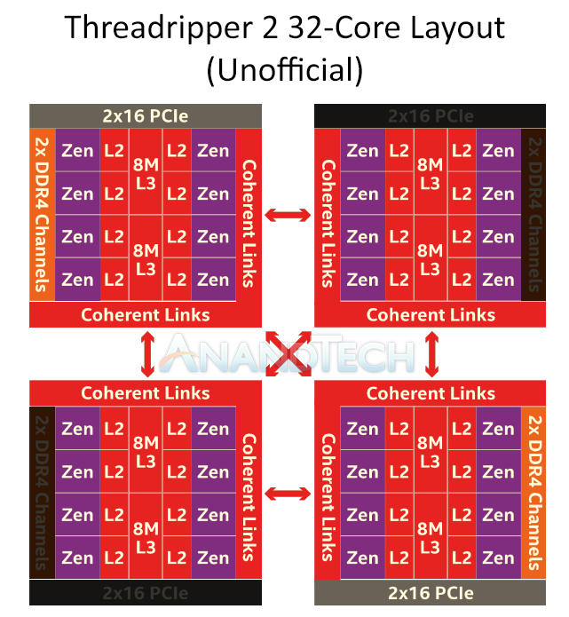
I'd love to get my hands on such a demo. Can you give details on it? What language/dependencies? Are you likely to share the source? As for the 32 core clock and boost.. I think you need to remind yourself that this is 32 cores... My current 1950x runs at 250W TDP when maxed out with just a mild OC above stock speeds. You're spreading this (even w/ power reductions of 12nm) across double the amount of cores. It's a slightly cut down 32 core epyc :
https://www.newegg.com/Product/Product.aspx?Item=N82E16819113471
which runs at 2.7/3.2
You're already seeing the (12nm) at work given that you'r getting 3.0/3.4.. maybe slap on another 300-500Mhz max for an intel housefire like TDP (which is probably why new beefier VRM threadripper boards have arrived). I'm not sure what kind of arrangement people have but OC'ing dumps an incredible amount of unnecessary heat from one's setup. If you're actually utilizing all of the I/O and have those PCIE slots slammed with cards, you're talking about a space heater when this thing gets going.
 

ub4ty

Senior member
Jun 21, 2017
749
898
96
Is AMD confirmed that memory arrangement? As they have 4 dies and 4-channel memory it is also easy to impelement 1-channel per die memory configuration which makes every die equal to each other instead of odd configuration of two dies with local memory only and two with far memory only.
I'd hope they would have detailed this at launch but my thinking is there is no way in hell two feed the other dies in this manner because I'm not sure you can have dynamic wiring to the dimm/pcie and I/O. This traces are fixed in the mobo to set pins. So, there's frankly no way to physically reach the two new dies besides power from the mobo. Someone correct me if i'm wrong
 

naukkis

Senior member
Jun 5, 2002
705
576
136
I'd hope they would have detailed this at launch but my thinking is there is no way in hell two feed the other dies in this manner because I'm not sure you can have dynamic wiring to the dimm/pcie and I/O. This traces are fixed in the mobo to set pins. So, there's frankly no way to physically reach the two new dies besides power from the mobo. Someone correct me if i'm wrong

They don't need dynamic wiring, they only need to route one memory channel from four dies in cpu substrate to memory channels instead of two channel from two dies. It's not a problem at all so that configuration with two dies without local memory is just so stupid solution that I think it's only from some journalist pen instead of AMD, or at least I hope so.
 

ub4ty

Senior member
Jun 21, 2017
749
898
96
Oh, one more thought here: They should have made 8 channel motherboards, while utilizing quad channel mode for older boards. That would provide an incentive to upgrade the board along with the chip. At any rate, anyone want to buy my 1950X, ASUS ROG Strix X399-E, 32 GB RAM? I can also throw in a broken MSI X399 carbon for good measure. :)
Something tells me just like with 1950x that the dies are sourced from EPYC dies that have defects in the I/O regions .. For 2 die config it's in the infinity fabric region. For this 4 die config its in the
- PCIE
- DDR4 mem controller
region. So, it would be physically impossible.

Otherwise, for dies w/ no defects, what you describe is just an EPYC chip. So, I don't think they would or could have done this. How did you break a mobo btw? *asking for a friend
 
Last edited:

ub4ty

Senior member
Jun 21, 2017
749
898
96
They don't need dynamic wiring, they only need to route one memory channel from four dies in cpu substrate to memory channels instead of two channel from two dies. It's not a problem at all so that configuration with two dies without local memory is just so stupid solution that I think it's only from some journalist pen instead of AMD, or at least I hope so.
*Route? There are physical board traces from the dimm slots to the pinouts on the CPU. When you say *routing* as in re-routing the data once its in a cpu complex that's essentially what is described here :
TR_Layout_Unofficial_AT_575px.png

The wire traces to the CPU pin outs are set. They aren't dynamic. Once the data is in the CPU complex you can re-route it sure but that's the problem were discussing and the latency therein. The above diagram is most likely 100% accurate save for the logistics on how the data routing is done. Suffice to say this is definitely a head scratcher and needs a range of use cases to proof its viability.
 

ub4ty

Senior member
Jun 21, 2017
749
898
96
New cooler (Cooler Master I think) designed for Threadripper.

dn18j0tm2e211.jpg
I'll stick w/ my Noctua. Although, I wish they had better mating of the heatpipes w/ the contact plate. Is a single fan wedged in between there it seems?
 

naukkis

Senior member
Jun 5, 2002
705
576
136
*Route? There are physical board traces from the dimm slots to the pinouts on the CPU. When you say *routing* as in re-routing the data once its in a cpu complex that's essentially what is described here :
TR_Layout_Unofficial_AT_575px.png

The wire traces to the CPU pin outs are set. They aren't dynamic. Once the data is in the CPU complex you can re-route it sure but that's the problem were discussing and the latency therein. The above diagram is most likely 100% accurate save for the logistics on how the data routing is done. Suffice to say this is definitely a head scratcher and needs a range of use cases to proof its viability.

Between CPU dies and motherboard is substrate which routes signals from dies to pins. There's no problem at all reconfigure those as wanted.
 

ub4ty

Senior member
Jun 21, 2017
749
898
96
Between CPU dies and motherboard is substrate which routes signals from dies to pins. There's no problem at all reconfigure those as wanted.
Interesting. Thank you for this bit of information. I was unaware of that. May you link me if possible?
I think more and more its clear to me for wait until official details come out.
 

The Stilt

Golden Member
Dec 5, 2015
1,709
3,057
106
Between CPU dies and motherboard is substrate which routes signals from dies to pins. There's no problem at all reconfigure those as wanted.

The CPU substrate isn't the problem, the topology of the existing motherboards is.
The existing boards are 2 DPC, A0 & A1, B0 & B1, C0 & C1 and D0 & D1 are sharing the signals.
 
  • Like
Reactions: Drazick and CatMerc

naukkis

Senior member
Jun 5, 2002
705
576
136
Interesting. Thank you for this bit of information. I was unaware of that. May you link me if possible?
I think more and more its clear to me for wait until official details come out.

It's just how flip-chips CPU's are made:

http://electronicpackaging.asmedigitalcollection.asme.org/article.aspx?articleid=2532707

That substrate dictates how die connects to cpu pins, it's normal to use one die to many different sockets. Intel did that recently with Kabylake, they used that same die with 2-channel socket 1150 substrate and with different substrate that same die could be used with 4-channel memory motherboard(LGA2066), of course only with 2-memory channels as die didn't have more. Same way AMD could wire 1-channel from 4 dies to memory channels with 4-die Threadrippers, and if they don't do it that way they are...... ?
 
  • Like
Reactions: ub4ty

naukkis

Senior member
Jun 5, 2002
705
576
136
The CPU substrate isn't the problem, the topology of the existing motherboards is.
The existing boards are 2 DPC, A0 & A1, B0 & B1, C0 & C1 and D0 & D1 are sharing the signals.

Every memory channel has two memory sockets, what's the problem?
 

TassadarL

Junior Member
Jun 6, 2018
4
2
16

CatMerc

Golden Member
Jul 16, 2016
1,114
1,149
136

ub4ty

Senior member
Jun 21, 2017
749
898
96
What I tested is I used dual channel 2933MHz RAM on Die#0 and no RAM on Die#1. Using compression test that Die#1 only perform 70% what Die#0 performed.
Very interesting and not bad. My question would be what happens when both dies try to suck through the same straw vs. one die at a time. Both dies drawing down on the dimm is more realistic (if the config is as described by anandtech) because if I max out all 32 cores you essentially have two dies now fighting for the same memory whereas in a proper epyc config with all dies individually fed, everyone has their own straw and pool to suck from.

I'm really enjoying the discussion on this and I'm learning alot. However, ultimately AMD should go in great detail on this issue as well as benchmarks and demonstrated use cases for how to most efficiently utilize this weird combo. I guess this gets resolved a bit if it is as Naukkis says and the dies get their own half straw?
 
  • Like
Reactions: CatMerc

CatMerc

Golden Member
Jul 16, 2016
1,114
1,149
136
As of right now, the 32 core Threadripper is clocked at 3.0 base and 3.4 boost. It looks like the 32 core version is finalized, but the 24 core version is not. This doesn't make sense given the improved PB2 + XFR changes. The boost should be up in the 4.2-4.3 ghz range. AMD really needs to work on their boosting algorithm. They would be doing a service to us all if they used a combination of a microcode update and a bios update to an enhanced PB + XFR offering. I've long suspected that the 'clock table' of the original Ryzen series was stored either in microcode or in the BIOS itself. The correct approach to this situation would be to monitor TDP via the active sensors and send clock up to the max boost clock as needed based on core usage and TDP. Doing so would enhance performance for older parts. This would require some work, both by AMD and by board manufacturers, but would create a ton of good will for AMD customers. It would also hurt Intel similarly, as in the past Intel has known to pull anti-consumer actions (such as attempting to charge for extra features, etc.).

Regardless, if they can get the max boost up to 2700X levels, I would consider buying the 32 core chip. As it stands, my overclocked 16 core Threadripper performs significantly better in games than the 1800X did, and pretty much ties up with a non overclocked 2700X, in some cases exceeding performance in places where cores/threads matter.

Finally, I've written a voxel tech demo that I may turn into a benchmark. It generates a world of X size and utilizes all cores. It also utilizes all cores when discarding/rendering chunks as the user moves around the world. It would be interesting to release this as a benchmark to see how well the future of gaming really compares when it comes to multi-core.
Neither are finalized. Both turbo numbers were listed as WIP. And were listed as ALL CORE turbo btw.
 

TassadarL

Junior Member
Jun 6, 2018
4
2
16
Very interesting and not bad. My question would be what happens when both dies try to suck through the same straw vs. one die at a time. Both dies drawing down on the dimm is more realistic (if the config is as described by anandtech) because if I max out all 32 cores you essentially have two dies now fighting for the same memory whereas in a proper epyc config with all dies individually fed, everyone has their own straw and pool to suck from.

I'm really enjoying the discussion on this and I'm learning alot. However, ultimately AMD should go in great detail on this issue as well as benchmarks and demonstrated use cases for how to most efficiently utilize this weird combo. I guess this gets resolved a bit if it is as Naukkis says and the dies get their own half straw?
This performance is too bad to function normally. If you use the same method on Games, use Die#1 to play game you can see a significant jumper frame time.I will test " both dies try to suck through the same straw" today with this situation. You can see EPYC as one single CPU as one DIE, 4 dies as 4 "cores", infinity fabric bus as "L3" which is sync to RAM speed. Then you can easily understand if TR2 with 4 "Cores" but only 2 memory controller looks like
 

TassadarL

Junior Member
Jun 6, 2018
4
2
16
Very interesting and not bad. My question would be what happens when both dies try to suck through the same straw vs. one die at a time. Both dies drawing down on the dimm is more realistic (if the config is as described by anandtech) because if I max out all 32 cores you essentially have two dies now fighting for the same memory whereas in a proper epyc config with all dies individually fed, everyone has their own straw and pool to suck from.

I'm really enjoying the discussion on this and I'm learning alot. However, ultimately AMD should go in great detail on this issue as well as benchmarks and demonstrated use cases for how to most efficiently utilize this weird combo. I guess this gets resolved a bit if it is as Naukkis says and the dies get their own half straw?
I used Single channel per die as system to test game, and set affinity on both dies like DIE 0 use 8 threads and DIE 1 use 8 threads together, the FPS was much worse than memory set 2+0
 

TassadarL

Junior Member
Jun 6, 2018
4
2
16
Very interesting and not bad. My question would be what happens when both dies try to suck through the same straw vs. one die at a time. Both dies drawing down on the dimm is more realistic (if the config is as described by anandtech) because if I max out all 32 cores you essentially have two dies now fighting for the same memory whereas in a proper epyc config with all dies individually fed, everyone has their own straw and pool to suck from.

I'm really enjoying the discussion on this and I'm learning alot. However, ultimately AMD should go in great detail on this issue as well as benchmarks and demonstrated use cases for how to most efficiently utilize this weird combo. I guess this gets resolved a bit if it is as Naukkis says and the dies get their own half straw?
Well the only one I desire or I concern is whether AMD give an 8-Channel desktop motherboard as X399-8ch or X499
 

The Stilt

Golden Member
Dec 5, 2015
1,709
3,057
106
Every memory channel has two memory sockets, what's the problem?

The fact that the signals are shared between the channels, outside the CAD and clock pins.
To support the individual channels each of the slots need to have their own signals routed on board.

The CPU (package) could do it, the socket obviously can do it but the existing motherboards cannot.
 

naukkis

Senior member
Jun 5, 2002
705
576
136
The fact that the signals are shared between the channels, outside the CAD and clock pins.
To support the individual channels each of the slots need to have their own signals routed on board.

The CPU (package) could do it, the socket obviously can do it but the existing motherboards cannot.

What signals are shared between channels? Even when two channels come from one die they both can work independently to each other so not much can be shared between them.

Do you mixed this to 8-channel system? Obviously x399 boards only have 4-channels but is there something that prevents using one channel per die(two memory slots for every channel as 2 dimms per channel) so every die could have local memory, and system could still be real SMT NUMA which cpu with no local attached memory could not be. If AMD's solution really is two dies without local memory that configuration would be unique to anything out there and should need very own complex performance optimizations to both OS and programs itself.
 

StinkyPinky

Diamond Member
Jul 6, 2002
6,763
783
126
They said that?

It is on Anandtech's website. Not sure if that is official or just speculation. They are samples also so it may be boosted slightly.

I'm also hoping for a new 16 core version with higher clocks and perhaps two dummy dies again.
 

eek2121

Platinum Member
Aug 2, 2005
2,930
4,025
136
It is on Anandtech's website. Not sure if that is official or just speculation. They are samples also so it may be boosted slightly.

I'm also hoping for a new 16 core version with higher clocks and perhaps two dummy dies again.

It amazes me how many people here browse the forums, but not the site. I am also hoping for a 16 core version, though if they can get the clocks up (if AT is wrong) then I'd consider a 24 or 32 core version.
 

The Stilt

Golden Member
Dec 5, 2015
1,709
3,057
106
What signals are shared between channels? Even when two channels come from one die they both can work independently to each other so not much can be shared between them.

Do you mixed this to 8-channel system? Obviously x399 boards only have 4-channels but is there something that prevents using one channel per die(two memory slots for every channel as 2 dimms per channel) so every die could have local memory, and system could still be real SMT NUMA which cpu with no local attached memory could not be. If AMD's solution really is two dies without local memory that configuration would be unique to anything out there and should need very own complex performance optimizations to both OS and programs itself.

Slots of the same memory channels (e.g. A0 & A1) share all but 10 signals (CAD).
You can look at any 2 DPC board schematic you can find, to check that.

Slots for the different channels (e.g. A0 & B0) share none, except the SMBUS ones for the SPD device.

All of the existing X399 boards with eight slots on them are 2 DPC (A0 & A1, B0 & B1, C0 & C1, D0 & D1), while an EPYC or 8CH TR would need to have 1 DPC (or 2 DPC with 16 slots) with A0, B0, C0, D0, E0, F0, G0, H0 configuration.

This is for a DDR3 board, but the DIMM type really makes no difference in this regard.

8UtHDtM.jpg


y2AE4AI.jpg