Discussion Packaging: EMIB, Infinity Fabric, CoWoS, Foveros

witeken

Diamond Member
Dec 25, 2013
3,899
193
106
I created this topic as a general packaging topic, but I will kick things of with EMIB.

Discussion

So I just had a discussion with Ian Cutress on Twitter, but things got heated up a bit lol. So just like EMIB removes the reticle size constraints, I hope this threads removes the character size constraints of Twitter.


The discussion started after Wikichip's latest packaging article: https://fuse.wikichip.org/news/2446/tsmc-demonstrates-a-7nm-arm-based-chiplet-design-for-hpc/

I asked a question about something in the article concerning EMIB's bump pitch, which it turns out I had misunderstood, but I also reasonably stated that Agilex was disclosed to use EMIB 2, which was slated to reduce the bump pitch from 55um to 35um, one-upping TSMC's 40um. (Later on, I also said that we're not really comparison apples to apples, since EMIB isn't an interposer.)

However, I got the surprising response that Agilex "doesn't exist", changing the discussion to a discussion about "when can you say something is real", since a product undergoes multiple stages from research to production (and clearly, Agilex is in initial production, proving that EMIB 2 is real).

However, while I was accused of "moving the goalposts", I was instead redirected to an earlier discussion, where Ian Cutress said he wanted to see "high-powered" dies connected to each other (I am not sure why that was suddenly relevant, so I simply pointed out that Agilex is quite high-powered already, and can be paired with custom silicon such as eASIC's), and also called in question the relevancy of that question.

So a discussion/question for clarification about bump pitches moved into a discussion about what sort of dies EMIB can connect, with Ian asking for proof for that. I 'cleverly' pointed out that Intel can't proof that since such products weren't on the roadmap for 2019.

---

So summing up the discussion:
  • Technical comparison of EMIB vs. CoWoS, including bump pitches, cost, advantages of EMIB over interposer, etc.
  • EMIB (2) in Agilex
  • What dies can EMIB connect? Proof of high-powered dies?
Summing up the facts:
  • EMIB shipping in Stratix 10 and Kaby Lake-G for years now
  • EMIB can have >20k bumps at 2Gbs, delivering well over 4TB/s; while CoWoS is 8Gbps, the disadvantage of higher rate is more complicated I/O circuits, EMIB uses simple I/O circuits
  • EMIB 2 (first seen in Agilex) reduces bump pitch from 55um to 35um, and 10um in the lab (note: 45um was shown on slide in Investor Meeting, not sure which EMIB version that referred to...)
  • Foveros = 36um bump pitch (in production with Lakefield by end of the year)
  • CoWoS = 40um bump pitch
  • Foveros, Intel's active interposer technology for 3D stacking, can handle up to 1kW power delivery
  • Power consumption: PCIe = 20pJ/bit, Infinity Fabric/package = 2pJ/bit die-to-die, CoWoS = 0.56pJ/bit, EMIB = 0.30pJ/bit, Foveros = 0.15pJ/bit, on-die = 0.1pJ/bit
Further about EMIB:
  • EMIB connections shipping: FGPA-Transceiver, FPGA-HBM, GPU-HBM
  • Also possible: Logic, ASIC, eASIC, RF, etc.
  • Intel claimed: splitting Xeon (= "high-powered") dies on 10nm++, Agilex can handle all sorts of chiplets including custom compute, Naveen Rao also came in and confirmed usage with Nervana
  • EMIB rumored: Arctic Sounds to use 2-4 GPU chiplets
  • EMIB leaked: Rocket Lake to use 14nm and 10nm graphics chiplets
  • Intel showed on Powerpoint (quote: David Schor):
"Compared to the single integrated circuit on the left, the product on the right consists of many xPUs on different process technologies optimized for their specific use-case. Those chips are then integrated onto a single package using 2D and 3D integration technologies such as EMIB and Foveros. For Intel, this means new technologies and capabilities can be developed independently and intercepted much earlier. Up to 2 years earlier according to Renduchintala. He added that compared to multi-chip packaging, “Foveros enables up to 10x increase in interconnect bandwidth while reducing the interconnect power by 6x at the same time.” One interesting remark made by Renduchintala is that this approach will allow Intel to selectively outsource various IPs that do help with product differentiation.

It’s difficult to know how much of the illustration shown is real and how much creative freedom was involved. If we were to scrutinize the drawing a little, we can see 4 chiplets sitting on some kind of interposer along with what appears to be four SRAM chips and another chip. There are four HBM stacks connected to each of those interposers. In total, there are four of those interposers interconnected using EMIBs for a total of 16 xPUs, 16 SRAM chips, 4 unknown chips, and 16 HBM stacks."

Naveen confirming EMIB/Foveros coming to Nervana:

https://twitter.com/NaveenGRao/status/1142596206775930880

I also asked for a Packaging Demonstration Day:

https://twitter.com/witeken/status/1142747213359132672

1561289834325.png

1561290000405.png
1561290047890.png
1561291404661.png
 
Last edited:

Abwx

Lifer
Apr 2, 2011
11,616
4,474
136
Summing up the facts:
  • EMIB shipping in Stratix 10 and Kaby Lake-G for years now
  • EMIB can have >20k bumps at 2Gbs, delivering well over 4TB/s; while CoWoS is 8Gbps, the disadvantage of higher rate is more complicated I/O circuits, EMIB uses simple I/O circuits
  • EMIB 2 (first seen in Agilex) reduces bump pitch from 55um to 35um, and 10um in the lab (note: 45um was shown on slide in Investor Meeting, not sure which EMIB version that referred to...)
  • Foveros = 36um bump pitch (in production with Lakefield by end of the year)
  • CoWoS = 40um bump pitch
  • Foveros, Intel's active interposer technology for 3D stacking, can handle up to 1kW power delivery
  • Power consumption: PCIe = 20pJ/bit, Infinity Fabric/package = 2pJ/bit die-to-die, CoWoS = 0.56pJ/bit, EMIB = 0.30pJ/bit, Foveros = 0.15pJ/bit, on-die = 0.1pJ/bit


View attachment 7647

View attachment 7648
View attachment 7649
View attachment 7650

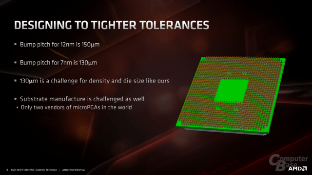
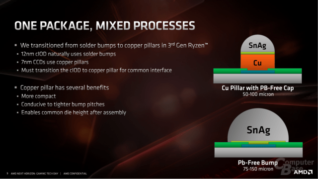
Summing facts that are irrelevants the ones with the others..

You are quoting IFabric at 2 pJ/bit while you are quoting Intel s power efficency solutions only for the microntact, that is, the micrometric bump.

AMD use bumps as small as 50um, so your numbers are obviously quasi stochastic since Intel quote 35um for their smaller height and a value of 0.15pJ/bit, wich should had ringed a bell when compared to an on die connection that is at 0.1pJ/bit.

1-630.256b8f39.png


2-630.fd90b976.png


4-630.a1d51560.png


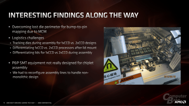
https://www.computerbase.de/2019-06/amd-zen-2-ryzen-3000-architektur/
 
  • Like
Reactions: ksec and piesquared

name99

Senior member
Sep 11, 2010
562
461
136
If we're going to get into a dick measuring contest regarding future packaging, it seems appropriate to mention that CoWoS is basically only TSMC's mid-level. At the lower level (kinda sorta) there is InFO, while at the top level (kinda sorta) there is SoIC
https://en.ctimes.com.tw/DispNews.asp?O=HK2AN94TZR6SAA00NZ

Significant points are
- mass production 2021
- stacked 3D
- <10µ bump pitch

Meanwhile even lowly InFO isn't standing still. InFO_MS has been qualified, and brings HBM to InFO. As far as I can tell (*very handwaving*!) TSMCs answer to many places where Intel would use EMIB is to slap down a fine pitch copper RDL, and it seems to be working for them.

Details of InFO_MS here:
https://semiengineering.com/more-2-5d-3d-fan-out-packages-ahead/
(Mark Lapedus says it's in R&D, but Cadence 9 months ago said it was qualified and ready to go as soon as a customer wanted it.)

The general point, I think, is that arguing over low-level details is stupid, like saying that one program is better than another because it was written in Rust rather than Swift. What matters is the capabilities of each of these techs, and by that metric
- TSMC seems to be marginally ahead in metrics by "very public" announcement
- INTC may be ahead by "kinda sorta announced, but not very publicly"
- INTC is shipping some EMIB stuff, sure. But AMD is also shipping a whole lot of traditional interposer stuff, and seems to be doing OK.

- MOST of the discussion seems to be "my team, therefore rah rah", and unfortunately we don't seem to have data to go much beyond that, or (the REAL problem...) any sort of agreement on what the actual goals are. CoWoS and InFO are used in vast numbers of products today (all those iPhones), extraordinary packaging is used in Apple Watches, and AMD are chugging along just fine.

I'd suggest, as at least one attempt to kinda sorta compare apple's with apples, that we look closely at Lakefield, when it arrives, compared with at the least the A12X and, hopefully, an A13X if there is one. Both are attempting to solve more or less the same problem, tablet-level compute, big and little cores, and A12X does something strange (I've seen no deeper analysis...) with the packaging of the DRAM on the die.
IF there's some spectacular metric associated with Lakefield, then advantage EMIB+Foveros. But otherwise, let the EMIB partisans accept that EMIB is just a means to an end, an end that's apparently achieved just as well by other companies using other means.


Oh, one last thing. Intel seems to be more and more in the business of announcing stuff that's three to five years away, whereas most of what TSMC announces is either working or a year away. (The SoIC stuff is two years away, but they're not yet making a big deal about it). Be very careful when you compare company A's 2019Q4 product specs with company B's 2022Q4 product specs.
 

NTMBK

Lifer
Nov 14, 2011
10,349
5,427
136
Oh, one last thing. Intel seems to be more and more in the business of announcing stuff that's three to five years away, whereas most of what TSMC announces is either working or a year away. (The SoIC stuff is two years away, but they're not yet making a big deal about it). Be very careful when you compare company A's 2019Q4 product specs with company B's 2022Q4 product specs.

Yup... Intel is starting to sound like Globalfoundries did about 5 years ago. It's not a great sign.
 
  • Like
Reactions: Lodix

jpiniero

Lifer
Oct 1, 2010
15,473
5,951
136
Yup... Intel is starting to sound like Globalfoundries did about 5 years ago. It's not a great sign.

Yeah. I wouldn't be surprised if AMD beats Intel to Active Interposer in servers, the way things are going.
 

witeken

Diamond Member
Dec 25, 2013
3,899
193
106
Yup... Intel is starting to sound like Globalfoundries did about 5 years ago. It's not a great sign.
Uhm. Intel did this because the tech community asked it, was tired of 3-4 yrs of Skylake.

Lakefield is coming this year or early next year, so a year at most.

Remember the difference between announcement and production of 10nm? Silicon photonics? 3DXPoint? 3D NAND? Discrete GPU?

This is nothing new.
 

DrMrLordX

Lifer
Apr 27, 2000
22,280
12,028
136
@name99

Lakefield may have pretty limited release and may be hampered by underlying problems with the 10nm process (clockspeeds). A teardown of Lakefield will tell us some of what Intel can do with their packaging technology, but it won't tell us the entire story. Apple is still able to design monolithic dice on the latest TSMC nodes and ship working products. Intel can only barely ship anything on their latest node (10nm). We can't really look at Foveros in isolation.

If Intel were launching (for example) a desktop 16c Ice Lake-S processor featuring 4 4c dice connected by EMIB and/or Foveros then that would be really something, and we could maybe compare it to upcoming chips like AMD's 3950x. As it stands, Intel isn't doing much with their packaging tech . . .yet.
 

name99

Senior member
Sep 11, 2010
562
461
136
@name99

Lakefield may have pretty limited release and may be hampered by underlying problems with the 10nm process (clockspeeds). A teardown of Lakefield will tell us some of what Intel can do with their packaging technology, but it won't tell us the entire story. Apple is still able to design monolithic dice on the latest TSMC nodes and ship working products. Intel can only barely ship anything on their latest node (10nm). We can't really look at Foveros in isolation.

If Intel were launching (for example) a desktop 16c Ice Lake-S processor featuring 4 4c dice connected by EMIB and/or Foveros then that would be really something, and we could maybe compare it to upcoming chips like AMD's 3950x. As it stands, Intel isn't doing much with their packaging tech . . .yet.

Remember that Apple IS using TSMC tech for PoP packaging of DRAM stacked on A12, and something else (as I said, details unclear) for DRAM packaging on the A12X die. These may not be interposer packaging, but that's kinda my point --- there are MANY interesting aspects to packaging.

I do agree with your analysis of Lakefield (it's a crazy product that in any sane universe would be a single die, and the fact that it isn't shows how bad 10nm is, not how great Foveros is) and have said so elsewhere; but it's also all we have available this year to compare against.
So, like I said: the fans insist on comparing what TSMC has available today with what Intel will one day have available at some point in the magical future...

The basic problem is one of credibility. If Intel insists on telling us stories about 10nm that strain credulity, why should we believe that EMIB is this great leap forward unmatched by any other company?
 

IntelUser2000

Elite Member
Oct 14, 2003
8,686
3,786
136
I do agree with your analysis of Lakefield (it's a crazy product that in any sane universe would be a single die, and the fact that it isn't shows how bad 10nm is, not how great Foveros is)

Actually, Foveros is what enables the advantages in Lakefield so unlike their other product lines its not merely there to ease transition to new process technologies but has a real benefit.

Unlike other chips, development sounded like it happened much later and it was planned for it. A customer asked for it in 2016!
 

DrMrLordX

Lifer
Apr 27, 2000
22,280
12,028
136
Remember that Apple IS using TSMC tech for PoP packaging of DRAM stacked on A12, and something else (as I said, details unclear) for DRAM packaging on the A12X die. These may not be interposer packaging, but that's kinda my point --- there are MANY interesting aspects to packaging.

What advantage did Apple gain from using TSMC's PoP packaging for stacked DRAM? Honest question. I haven't seen much commentary on the subject.
 

IntelUser2000

Elite Member
Oct 14, 2003
8,686
3,786
136
What advantage did Apple gain from using TSMC's PoP packaging for stacked DRAM? Honest question. I haven't seen much commentary on the subject.

PoP stands for Package-on-Package. It's just for saving space. It's been used on mobile SoCs for years. Lakefield also uses PoP. Earliest use for Intel was Medfield. The simplicity also reduces cost and has a fast turnaround time.
 

NTMBK

Lifer
Nov 14, 2011
10,349
5,427
136
What advantage did Apple gain from using TSMC's PoP packaging for stacked DRAM? Honest question. I haven't seen much commentary on the subject.

Smaller motherboard, leaves room for a bigger battery.
 

DrMrLordX

Lifer
Apr 27, 2000
22,280
12,028
136
PoP stands for Package-on-Package. It's just for saving space. It's been used on mobile SoCs for years. Lakefield also uses PoP. Earliest use for Intel was Medfield. The simplicity also reduces cost and has a fast turnaround time.

Smaller motherboard, leaves room for a bigger battery.

Okay, that's what I thought. Thanks for verification.

In that light, I don't see Apple's (or anyone else's) use of PoP to be in the same ballpark as Intel's reliance on Foveros in Lakefield. At the very least, it's nowhere near as radical a design decision.
 

IntelUser2000

Elite Member
Oct 14, 2003
8,686
3,786
136
In that light, I don't see Apple's (or anyone else's) use of PoP to be in the same ballpark as Intel's reliance on Foveros in Lakefield. At the very least, it's nowhere near as radical a design decision.

Intel kinda needs it. They are like freight trucks in terms of maneuverability. Maybe because of lot of layers in the company that slows things down? I don't know.

If they have something like the 6-series chipset bug, on Foveros it would be on a separate stack and would have faster response times than if they were on-die. Actually, if it was on-die and it had a bug, the product is done. I can't imagine how long it would take for them to reiterate it.

So its more of allowing x86 devices to expand than being a direct threat to ARM. Trying to enter Android market is a lost cause anyway.
 
  • Like
Reactions: DarthKyrie

DrMrLordX

Lifer
Apr 27, 2000
22,280
12,028
136
Intel kinda needs it.

Indeed they do! Intel can barely fab anything on 10nm. I don't think Lakefield could ever work if they tried making a monolithic die with I/O + SoC functions, compute cores, and GPU all on the same die. I'm curious what else they've done to tie the whole package together . . .
 

name99

Senior member
Sep 11, 2010
562
461
136
Actually, Foveros is what enables the advantages in Lakefield so unlike their other product lines its not merely there to ease transition to new process technologies but has a real benefit.

Unlike other chips, development sounded like it happened much later and it was planned for it. A customer asked for it in 2016!

What ARE those advantages compared to simply creating a monolithic die?
You can't have it both ways, saying that Lakefield is less performant than A12X because A12X is monolithic AND that Foveros provides unique advantages...

Both LakeField dies are tiny. There's no reason the pair could not be monolithic if 10nm is yielding well.
 

IntelUser2000

Elite Member
Oct 14, 2003
8,686
3,786
136
What ARE those advantages compared to simply creating a monolithic die?
You can't have it both ways, saying that Lakefield is less performant than A12X because A12X is monolithic AND that Foveros provides unique advantages...

If you were keeping track of Intel products, you may know.

Also, I never compared it to ARM-based cores at all, including Apple's. The main benefactor is Intel. I have a feeling you probably skimmed through or skipped the last few posts.

Post #15 described Intel's "unique" issue.

They need an on-die chipset solution because that's likely the reason why they are still quite behind in the battery life department(once you normalize to WHr). Foveros allows it to avoid the issues in #15, while making it work like on-die.
 

name99

Senior member
Sep 11, 2010
562
461
136
PoP stands for Package-on-Package. It's just for saving space. It's been used on mobile SoCs for years. Lakefield also uses PoP. Earliest use for Intel was Medfield. The simplicity also reduces cost and has a fast turnaround time.

Traditional PoP stacks the DRAM on the SoC using wires that are micro-soldered from one to the other. See the picture here:
https://www.micron.com/about/blog/2015/march/the-mobile-package-just-got-smaller

As always with wires, this has a cost in RC (and it's slightly fragile).

Since A10 Apple has used InFO which is more like interposer type tech --3D, not 2.5D, but based on stacking dies with routing between the two done by a copper RDL, micro bumps, and (perhaps? it's unclear if Apple is using these) TSVs.

You can see pictures of various InFO options here
https://www.ansys.com/blog/tsmcs-info-packaging-technology
(note the LACK of the wires from one chip to another) and the Apple version here:
https://www.systemplus.fr/wp-content/uploads/2018/02/SP18373-Apple-A11-inFO-Packaging_Flyer.pdf

A12X is something else again. Look at the pictures here:
https://semimd.com/chipworks/2019/01/16/the-packaging-of-apples-a12x-is-weird/
Very unusual! Not a traditional PoP setup with wires. Not an InFO setup with stacked dies.
Looks like an interposer setup with the SoC and DRAM paced right next to each other on top of a sliver of common silicon.
The analysis of the article above is probably correct -- A12X doesn't need a "real" interposer, so this is kinda a poor man's interposer that gives you low RC and thermal advantages, without requiring the fancy RDL of a "real" interposer. But it's definitely cute, and suggests that Apple may investigating both more aggressive 3D stacking (iPhone side, plus aWatch) AND 2.5D techniques (iPad side, to be followed by ARM macs?)
 

name99

Senior member
Sep 11, 2010
562
461
136
Okay, that's what I thought. Thanks for verification.

In that light, I don't see Apple's (or anyone else's) use of PoP to be in the same ballpark as Intel's reliance on Foveros in Lakefield. At the very least, it's nowhere near as radical a design decision.

The place to look for truly aggressive Apple packaging is not the Phone (though there are very interesting techniques as I've described, along with a folder motherboard) but the Apple Watch.
The X-ray images clearly show something amazing going on there in terms of multiple stacked dies of all types,
https://www.ifixit.com/Teardown/Apple+Watch+Series+4+Teardown/113044
but no-one as far as I know has dared to go further in taking apart the SiP (the System in Package that's the real heart of the watch).
 
  • Like
Reactions: Lodix

IntelUser2000

Elite Member
Oct 14, 2003
8,686
3,786
136
The place to look for truly aggressive Apple packaging is not the Phone

Actually they did some amazing work on the board side with the iPhones.

Considering that Intel revealed they planned EMIB and Foveros back in 2016 I wonder what we would have had by now? They stood still on the technology for 3 years!
 

DrMrLordX

Lifer
Apr 27, 2000
22,280
12,028
136
What ARE those advantages compared to simply creating a monolithic die?

Intel can't produce a monolithic die. Not on 10nm, not with CPU + GPU + SoC functions + I/O. They're really that far up the creek.
 

maddie

Diamond Member
Jul 18, 2010
5,006
5,207
136
Last question and very interesting last two paragraphs in the answer.
https://www.anandtech.com/show/14568/an-interview-with-amds-forrest-norrod-naples-rome-milan-genoa

This is almost an inescapable effect of being so dominant. How can I continue to grow profits? You pretty much have to become very predatory. Same is happening with Nvidia. Not P&N but anyone see similarities to the wider world. Similar dynamics at play. Strangely enough, this behavior pretty much guarantees your failure longer term. Market reaction.


IC: Intel has extended out to all the other aspects of the enterprise market in order addressing more TAM than ever before, because that is the goal for investors. One of those aspects is volatile memory and Optane. What can AMD do in this space, or is it worth it the customers that you're going for to do some sort of non-volatile memory?

Forrest Norrod: With all these forms of NVM I do think that there are two value propositions that people have been talking about.

One is the non-volatile aspect, to blur the lines between memory and storage, and customers will get much better large memory database machines etc. On the whole non-volatile aspect, I think people are doing the software work to enable that on a broader range of applications, but at the end of the day, the fact that you still have a failure domain at the node level means that the value is relatively smaller. Before you can commit, you're going to trust a commit to just one machine, to the SCM on one machine. However realistically you're not going to commit until you got a commit on multiple nodes. And so, that tends to somewhat degrade the value that people were thinking about.

So the other aspect of course is lower cost per bit. They’ll use it as DRAM replacement and the fact is that it has longer latency and non-uniform latency, and so there are a bunch of issues there. Now withstanding that it is close enough that we can use it as DRAM replacement, I'd say there was probably more interest in that 12 months ago when DRAM price were at a historically high level. Today there is less interest in that now as DRAM prices have come way down and I do think that DRAM/memory is a commodity market, and commodity markets have a very set of economic rules. The cure for high oil prices is high oil prices right? You know because that increases production and that brings the oil prices back down. The prospect of Optane being a replacement for DRAM in of itself would bring the cost of DRAM down, regardless of the current market factors in play today.

But there are a lot of other storage class memory (SCM) technologies which are in development. I think that you will see SCM settle into a niche of the memory hierarchy over 2-3 years and I think that there will be a lot of choices, not just Optane. But I don't think it's the be-all and end-all. I think that that Intel has made a horrific mistake hitching their system architecture to a propriety memory interface. I think that they've made a key strategic mistake.

I think that in general, Intel may be forgetting what got them here. Truly having an open ecosystem where others could add value to that ecosystem, and that the platform is a key part of the success of the x86 market. Intel still talks about it in that way, but that's not what they are doing, any pico-acre of silicon that doesn't belong to Intel is something that they covet. But I think acting that way is to the detriment of the health of their platform ecosystem long term.
 
  • Like
Reactions: name99

lobz

Platinum Member
Feb 10, 2017
2,057
2,856
136
Uhm. Intel did this because the tech community asked it, was tired of 3-4 yrs of Skylake.

Lakefield is coming this year or early next year, so a year at most.

Remember the difference between announcement and production of 10nm? Silicon photonics? 3DXPoint? 3D NAND? Discrete GPU?

This is nothing new.
3DXPoint is NOTHING EVEN REMOTELY CLOSE like what was announced and hyped for 2 years.
 

dahorns

Senior member
Sep 13, 2013
550
83
91
3DXPoint is NOTHING EVEN REMOTELY CLOSE like what was announced and hyped for 2 years.

That's a pretty strong exaggeration. You could say 3DXpoint products aren't what was promised, but the technology itself appears to be exactly what was promised. And I expect that at some point you'll see products getting quite a bit closer to those theoretical performance numbers.