- Mar 3, 2017
- 1,601
- 5,780
- 136
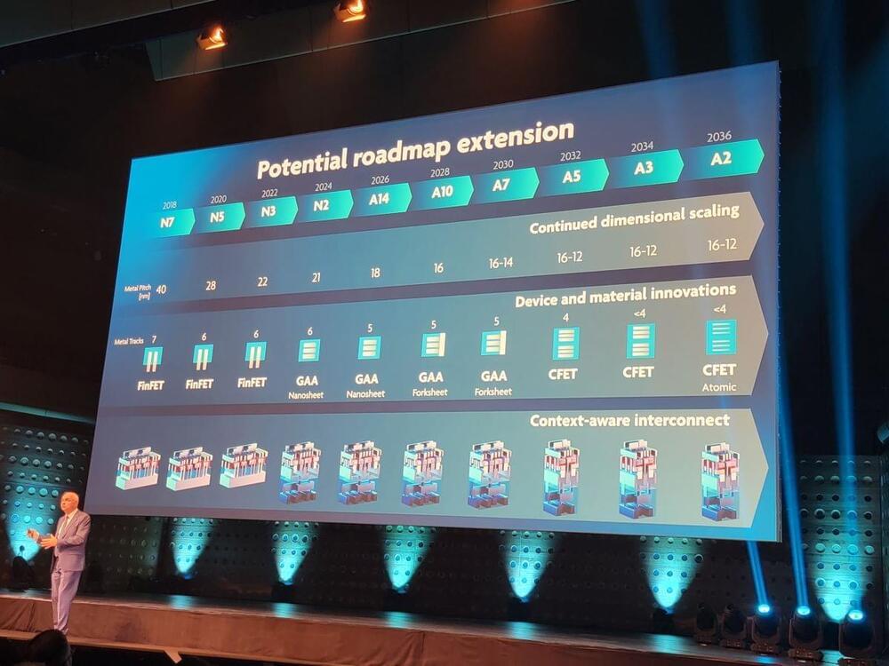
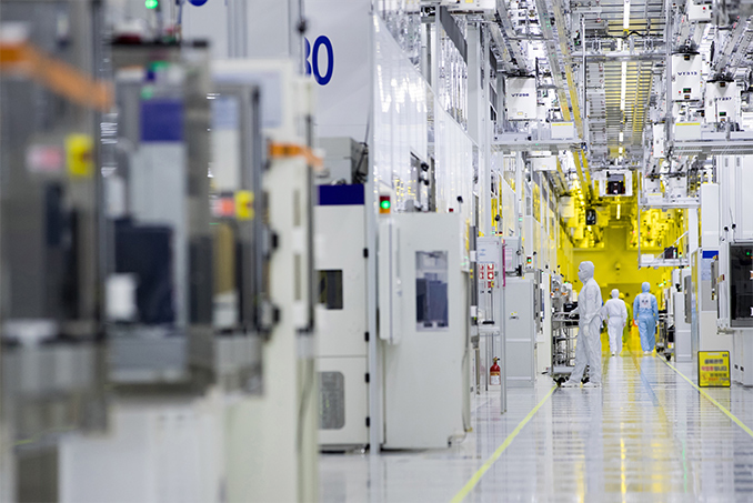
TSMC's N7 EUV is now in its second year of production and N5 is contributing to revenue for TSMC this quarter. N3 is scheduled for 2022 and I believe they have a good chance to reach that target.

N7 performance is more or less understood.

This year and next year TSMC is mainly increasing capacity to meet demands.
For Samsung the nodes are basically the same from 7LPP to 4 LPE, they just add incremental scaling boosters while the bulk of the tech is the same.
Samsung is already shipping 7LPP and will ship 6LPP in H2. Hopefully they fix any issues if at all.
They have two more intermediate nodes in between before going to 3GAE, most likely 5LPE will ship next year but for 4LPE it will probably be back to back with 3GAA since 3GAA is a parallel development with 7LPP enhancements.
 www.anandtech.com

Samsung's 3GAA will go for HVM in 2022 most likely, similar timeframe to TSMC's N3.
There are major differences in how the transistor will be fabricated due to the GAA but density for sure Samsung will be behind N3.
But there might be advantages for Samsung with regards to power and performance, so it may be better suited for some applications.
But for now we don't know how much of this is true and we can only rely on the marketing material.
This year there should be a lot more available wafers due to lack of demand from Smartphone vendors and increased capacity from TSMC and Samsung.
Lots of SoCs which dont need to be top end will be fabbed with N7 or 7LPP/6LPP instead of N5, so there will be lots of wafers around.
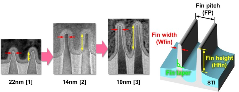
Most of the current 7nm designs are far from the advertized density from TSMC and Samsung. There is still potential for density increase compared to currently shipping products.
N5 is going to be the leading foundry node for the next couple of years.
For a lot of fabless companies out there, the processes and capacity available are quite good.
N7 performance is more or less understood.
This year and next year TSMC is mainly increasing capacity to meet demands.
For Samsung the nodes are basically the same from 7LPP to 4 LPE, they just add incremental scaling boosters while the bulk of the tech is the same.
Samsung is already shipping 7LPP and will ship 6LPP in H2. Hopefully they fix any issues if at all.
They have two more intermediate nodes in between before going to 3GAE, most likely 5LPE will ship next year but for 4LPE it will probably be back to back with 3GAA since 3GAA is a parallel development with 7LPP enhancements.
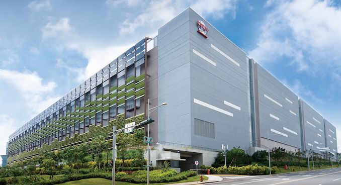
Samsung’s Aggressive EUV Plans: 6nm Production in H2, 5nm & 4nm On Track
Samsung's 3GAA will go for HVM in 2022 most likely, similar timeframe to TSMC's N3.
There are major differences in how the transistor will be fabricated due to the GAA but density for sure Samsung will be behind N3.
But there might be advantages for Samsung with regards to power and performance, so it may be better suited for some applications.
But for now we don't know how much of this is true and we can only rely on the marketing material.
This year there should be a lot more available wafers due to lack of demand from Smartphone vendors and increased capacity from TSMC and Samsung.
Lots of SoCs which dont need to be top end will be fabbed with N7 or 7LPP/6LPP instead of N5, so there will be lots of wafers around.
Most of the current 7nm designs are far from the advertized density from TSMC and Samsung. There is still potential for density increase compared to currently shipping products.
N5 is going to be the leading foundry node for the next couple of years.
For a lot of fabless companies out there, the processes and capacity available are quite good.