Discussion Intel Meteor, Arrow, Lunar & Panther Lakes Discussion Threads

Page 6 - Seeking answers? Join the AnandTech community: where nearly half-a-million members share solutions and discuss the latest tech.

Tigerick

Senior member
Apr 1, 2022
655
537
106
PPT1.jpg
PPT2.jpg
PPT3.jpg


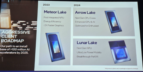
As Hot Chips 34 starting this week, Intel will unveil technical information of upcoming Meteor Lake (MTL) and Arrow Lake (ARL), new generation platform after Raptor Lake. Both MTL and ARL represent new direction which Intel will move to multiple chiplets and combine as one SoC platform.

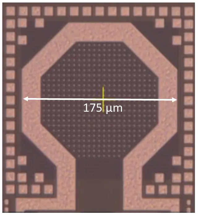
MTL also represents new compute tile that based on Intel 4 process which is based on EUV lithography, a first from Intel. Intel expects to ship MTL mobile SoC in 2023.

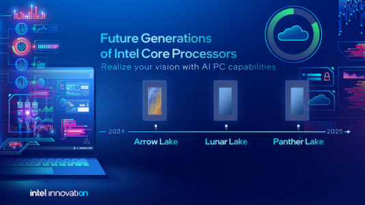
ARL will come after MTL so Intel should be shipping it in 2024, that is what Intel roadmap is telling us. ARL compute tile will be manufactured by Intel 20A process, a first from Intel to use GAA transistors called RibbonFET.


Comparison of upcoming Intel's U-series CPU: Core Ultra 100U, Lunar Lake and Panther Lake

ModelCode-NameDateTDPNodeTilesMain TileCPULP E-CoreLLCGPUXe-cores
Core Ultra 100UMeteor LakeQ4 202315 - 57 WIntel 4 + N5 + N64tCPU2P + 8E212 MBIntel Graphics4
?Lunar LakeQ4 202417 - 30 WN3B + N62CPU + GPU & IMC4P + 4E08 MBArc8
?Panther LakeQ1 2026 ??Intel 18A + N3E3CPU + MC4P + 8E4?Arc12


Comparison of die size of Each Tile of Meteor Lake, Arrow Lake, Lunar Lake and Panther Lake

Meteor LakeArrow Lake (20A)Arrow Lake (N3B)Arrow Lake Refresh (N3B)Lunar LakePanther Lake
PlatformMobile H/U OnlyDesktop OnlyDesktop & Mobile H&HXDesktop OnlyMobile U OnlyMobile H
Process NodeIntel 4Intel 20ATSMC N3BTSMC N3BTSMC N3BIntel 18A
DateQ4 2023Q1 2025 ?Desktop-Q4-2024
H&HX-Q1-2025
Q4 2025 ?Q4 2024Q1 2026 ?
Full Die6P + 8P6P + 8E ?8P + 16E8P + 32E4P + 4E4P + 8E
LLC24 MB24 MB ?36 MB ??8 MB?
tCPU66.48
tGPU44.45
SoC96.77
IOE44.45
Total252.15


Intel Core Ultra 100 - Meteor Lake

INTEL-CORE-100-ULTRA-METEOR-LAKE-OFFCIAL-SLIDE-2.jpg

As mentioned by Tomshardware, TSMC will manufacture the I/O, SoC, and GPU tiles. That means Intel will manufacture only the CPU and Foveros tiles. (Notably, Intel calls the I/O tile an 'I/O Expander,' hence the IOE moniker.)

Clockspeed.png
 

Attachments

  • PantherLake.png
    PantherLake.png
    283.5 KB · Views: 23,959
  • LNL.png
    LNL.png
    881.8 KB · Views: 25,428
Last edited:

Joe NYC

Golden Member
Jun 26, 2021
1,943
2,283
106
Keeping this related to Meteor/Arrow, what I want to know how the timing is going to work. If Meteor's going to be an EOY 23/24 product now, should we just assume that Arrow will be pushed back to EOY 24/25? They could just fill the rest of 14th Gen with Raptor Lake rebrands if need be.

Arrow Lake is (inexplicably) skipping "Intel 3" node, jumping 2 notes forward.

So it is sort of a Hail Mary, probably not really worth discussing time lines at this point.

Following what Gelsinger says, you would expect "Intel 3" to be ready shortly after "Intel 4" which would enable Intel to not only use it for CPU chiplet, but bring more chiplets hack in-house.

But it is not happening. It seems Intel is planning these big leaps, rather than having "normal" steps.
 
  • Like
Reactions: Vattila

Exist50

Platinum Member
Aug 18, 2016
2,445
3,043
136
We were talking about how AMD is "reaping low static power draw". At idle it matters very much how the layout of components is set up that you can completely turn off. For multicore CPUs it's the interconnect and cache hierarchy, especially LLC, that need to stay powered on even if the cores themselves are mostly shut down both to retain the data and to reduce latency once data is requested again.
Ok, so what do you claim AMD is actually doing differently there? It seems very weird to be having this conversation about MTL, which explicitly includes a way to power off most of the cores, the ring, and the LLC even without going into deep idle modes.
Since AMD introduced CCX with Zen the interesting part about their interconnect is that it's no longer distinctly visible (to the point that before Zen 3 we never got an official confirmation how the actual routing looks like) but designed as part of the L3 LLC.

Meanwhile Intel keeps spending plenty die area just for the interconnect, with the LLC in some designs as the mesh fabric being situated relatively far off of the actual cores.
When you look at the "ring" on an Intel die, most of what you're actually seeing is the LLC and the coherency agents. Again, I'm not sure how/why you think this is materially different from what AMD's doing.
The MTL compute die shots so far make it look like a direct continuation of the layout used in the previous generations, this time just on a disaggregated die.
The entire SoC die is radically different, and there are assuredly changes to the ring as well. Pretty much the only thing untouched is the fact that a ring still exists, but again, AMD now has that too, so...
But the old design still used is known to not scale all too well (which is why Intel trialed multiple rings before going with a mesh fabric for higher core counts). And meanwhile, imo visibly starting with Renoir, AMD suddenly passed Intel in low static power draw while Intel's mobile chips for the last couple generations actually manage to get worse there. That for Zen 3 (8c CCX and V-Cache) AMD admitted to be using some form of ring bus just further underlines that execution matters. So far I'm still not seeing Intel investing in research in that particular area.
About a decade later, we're only just now reaching the same number of ring stops that Broadwell had. Yes, it doesn't scale indefinitely, and eventually they will either need to add another die, or change topology, but none of that explains Alder Lake.
IF is not just the mainband fabric.
That's kind of my point. Comparing Infinity Fabric to Intel's ring bus as talking about power management is like discussing the relative suitability of an apple vs a block of wood for making a meatloaf. It just doesn't make sense.
 
  • Like
Reactions: Vattila

Exist50

Platinum Member
Aug 18, 2016
2,445
3,043
136
Do we know for certain that it is the same generation of e-core?
No, that's from me. I have extremely high confidence in what I said, but if you want to assume otherwise, doesn't really matter. Happy to wait for my claims to be proven.
But then, why in the world would Intel duplicate them on CPU die, just to get a better Cinebench score?
It seems like Intel is trying to use Atom cores for two very different things at once. On the SoC die, they're for low power compute, while on the compute die, they're for MT performance. Ideally they'd have a core optimized for each, but clearly that's out of scope for now.
This limitation was the necessity drove the partition decisions. Whether it turns out to also be a virtue as well remains to be seen.
Well if it's truly necessary to get a product out the door, I think any decision on incremental cost is moot.
Remains to be seen. It may need additional steps to fill the gap, or add support to the die. Bigger core chiplet may need additional power delivery to the rest of the die.

Let's compare this with client Zen 3, for example, where there is one type of substrate, it does not have to change to accommodate a 2nd chiplet, 2nd chiplet is identical replica of the 1st.

Intel has to redesign the chiplet to get more cores and also, possibly redesign the interposer. So the re-use is quite limited.
There's no reason to believe there's any issue with a superset die. By way of analogy, the same socket can support all sorts of dies today. At most, they'll need some dummy dies for assembly.

And I find the comparison to AMD odd. They effectively have 3 desktop packages - 1 or 2 compute dies connected to a superset IO die, or the mobile die for mainstream. In theory, Intel could have one base die to support a range of different compute dies without issue. I don't think they'll do that (because interposers are easy), but it should be possible. Anyway, not seeing a substantial difference in overhead there.
You would want much less in terms of packaging losses than to counteract the gains from individual binning of good dies. Because if you just break even, you could have made a monolithic chip. Which Intel could not.

So arguing from the other end, that since Intel chose the approach, it must be good ignores the fact that Intel had no other choice..
Traditionally, packaging losses are typically very low. You want like 99%+ yield. I don't have numbers for Foveros, but again, we have no reason (leak, rumor, etc) to believe it's an issue, so while we also don't yet have proof that it isn't, this logic seems like a dead end for now. Russel's teacup and all that.
 

Exist50

Platinum Member
Aug 18, 2016
2,445
3,043
136
With "tiles", one might think that a tile can communicate only with adjacent tile. But in case of Meteor Lake, using interposer, any "tile" can communicate with any other.
On MTL, it's only directional links with the SoC die. The GPU can't talk directly to the CPU, for instance.
There may be a plan B (C, D, E) in place to move the CPU chiplet at TSMC as well, if "Intel 4" is not ready. Which would be another advantage of chiplet approach.
Isn't that basically what ARL is? If they have the CPU tile on N3, that's full TSMC right there.
Following what Gelsinger says, you would expect "Intel 3" to be ready shortly after "Intel 4" which would enable Intel to not only use it for CPU chiplet, but bring more chiplets hack in-house.
IF 20A is ready, it makes perfect sense to skip Intel 3. Why wouldn't they use the best available? And if that doesn't work out, there's also N3. Server can presumably cover any Intel 3 ramp needs.
 
  • Like
Reactions: Joe NYC

Exist50

Platinum Member
Aug 18, 2016
2,445
3,043
136
Keeping this related to Meteor/Arrow, what I want to know how the timing is going to work. If Meteor's going to be an EOY 23/24 product now, should we just assume that Arrow will be pushed back to EOY 24/25? They could just fill the rest of 14th Gen with Raptor Lake rebrands if need be.
Sounds reasonable, but man, what a boring 2023 this'll be, at least for desktop. And Zen 5 without any real competition for some months won't be terribly fun either.
 

Joe NYC

Golden Member
Jun 26, 2021
1,943
2,283
106
On MTL, it's only directional links with the SoC die. The GPU can't talk directly to the CPU, for instance.

This would particular to the implementation of MTL. But in theory, with interposer, 2 chiplets that are not adjacent could communicate.

Isn't that basically what ARL is? If they have the CPU tile on N3, that's full TSMC right there.

IF 20A is ready, it makes perfect sense to skip Intel 3. Why wouldn't they use the best available? And if that doesn't work out, there's also N3. Server can presumably cover any Intel 3 ramp needs.

Arrow Lake is shown on latest Intel slides as 20A.

Intel is not going to make money if they don't reap full benefit from the nodes they develop, and if their fabs are not full. Server parts on "Intel 3" are too low volume to fully pay for the node development.

Designing Arrow Lake CPU chiplet on 20A increases risk of the product slipping, while Intel 3 may already be healthy, while Intel fabs are not fully utilized...

1661634245262.png
 
  • Like
Reactions: Vattila

DrMrLordX

Lifer
Apr 27, 2000
21,629
10,841
136
Off topic, but: AMD has to launch something to the ODM next January for the next round of laptop models in any case. Dragon Range and Phoenix Point are next in the line. (Actual availability to end consumers will be the same story as every year regardless.)

I was under the impression that first up we'd see Dragon Range, with Phoenix Point maybe coming later? I've heard a lot more info about Dragon Range specifically. Kinda makes me wonder.

It is a big leap:
- new CPU core
- new GPU
- new process node

The optimistic timeline is beginning of 2023. Even if there is a minor slip, it should still launch before Meteor Lake.

I think Dragon Range will, for sure. But Meteor Lake's actual launch should also be viewed with some skepticism, so it's hard to say how many other products could be launched before Meteor Lake finally reaches the market.
 
  • Like
Reactions: Joe NYC

jpiniero

Lifer
Oct 1, 2010
14,591
5,214
136
Arrow Lake is shown on latest Intel slides as 20A.

Intel is not going to make money if they don't reap full benefit from the nodes they develop, and if their fabs are not full. Server parts on "Intel 3" are too low volume to fully pay for the node development.

Might be a sunk cost deal because the R&D was done a long time ago. Intel 3 is really just 7+ and (regardless of what Intel's said on the topic) I have a feeling that 20A is really 7++. And given that 7 nm was supposed to be in HVM 2 years ago, you'd have to think the node definitions got to be older than that.

I also assume that the tooling is the same between the three.
 
  • Like
Reactions: ftt and Joe NYC

Doug S

Platinum Member
Feb 8, 2020
2,260
3,511
136
Arrow Lake is (inexplicably) skipping "Intel 3" node, jumping 2 notes forward.

So it is sort of a Hail Mary, probably not really worth discussing time lines at this point.

Following what Gelsinger says, you would expect "Intel 3" to be ready shortly after "Intel 4" which would enable Intel to not only use it for CPU chiplet, but bring more chiplets hack in-house.

But it is not happening. It seems Intel is planning these big leaps, rather than having "normal" steps.


Isn't Intel 3 planned to be their first big leading edge foundry node offering? Maybe they don't want in house to compete with foundry so they're skipping it?
 

Exist50

Platinum Member
Aug 18, 2016
2,445
3,043
136
Arrow Lake is shown on latest Intel slides as 20A.
Ah, but it's also external. Funny how much wiggle room those slides leave.
Intel is not going to make money if they don't reap full benefit from the nodes they develop, and if their fabs are not full. Server parts on "Intel 3" are too low volume to fully pay for the node development.
Eh? Server will put a ton of volume onto Intel 3. And I'm sure it'll also be popular for IO dies and the like.
Intel 3 is really just 7+ and (regardless of what Intel's said on the topic) I have a feeling that 20A is really 7++.
It would be more accurate to think of Intel 4 as 7+ (original 7 being the canceled Ponte Vecchio node), Intel 3 as being 7++, and Intel 20A being 5.
 

shady28

Platinum Member
Apr 11, 2004
2,520
397
126
Might be a sunk cost deal because the R&D was done a long time ago. Intel 3 is really just 7+ and (regardless of what Intel's said on the topic) I have a feeling that 20A is really 7++. And given that 7 nm was supposed to be in HVM 2 years ago, you'd have to think the node definitions got to be older than that.

I also assume that the tooling is the same between the three.

Intel 4 and Intel 3 are closely related.

I'm not an EE, but my take on the article below (also summary quote) is that Intel 4 is a stepping stone to ramp production and yield on EUV with limited libraries that are tailored specifically to Intel CPUs (server and client). The materials tech is also geared towards high-power use cases.

I would also assume this is why, for example, Intel is using TSMC for components other than the compute die for Meteor Lake.

Intel 3 appears to have both denser and broader use libraries, and possibly different materials, along with much greater efficiency. It would make sense that Intel would then have a top tier foundry node.

Along those lines, they are already moving into the more mundane area where they have 'Intel 16' node. That's a foundry node, not everyone needs expensive sub 5nm nodes. I believe Intel 16 is actually their 22nm node with FinFet, so they've completely adopted the TSMC/Samsung naming conventions (TSMC/Samsung/Gloflo 14/16nm nodes were 20nm + FinFet, whereas Intel's 14nm was a true node shrink + FinFet nearly equivalent to the other foundries "10nm\12nm" nodes).

As to Meteor Lake and Arrow Lake, I am not real enthused about them. I expect Meteor Lake will bring much higher multi-thread performance with its new E-cores, and probably much better iGPU performance, but I am not interested in either (some will be). Arrow Lake I expect will bring much higher power efficiency, great in the server space but really trivial to desktop users - might bring a lot to the mobile space though.


"Despite all of this, we consider Intel 4 a stopgap node – a minimum viable product; an interim node on the way to Intel 3 which is expected to ramp roughly a year after Intel 4 (late next year). Intel 3 will be the final FinFET process from Intel. Everything thereafter will utilize a new gate-all-around transistor architecture the company calls RibbonFET. "
 
  • Like
Reactions: Vattila

DrMrLordX

Lifer
Apr 27, 2000
21,629
10,841
136
It would make sense that Intel would then have a top tier foundry node.

Wishful thinking. We will see, but . . . probably not going to be "top tier" by the time you see any IFS customers actually use it.

I believe Intel 16 is actually their 22nm node with FinFet,

It appears to be an enhanced version of 22FFL which is a 14nm variant:

 
  • Like
Reactions: Vattila

mikk

Diamond Member
May 15, 2012
4,140
2,154
136
As to Meteor Lake and Arrow Lake, I am not real enthused about them. I expect Meteor Lake will bring much higher multi-thread performance with its new E-cores, and probably much better iGPU performance, but I am not interested in either (some will be). Arrow Lake I expect will bring much higher power efficiency, great in the server space but really trivial to desktop users - might bring a lot to the mobile space though.

Meteor Lake is limited to 6+8, the much higher multithread performance is more likely to come with Arrow Lake which reportedly gets a new 8+32 highend tile. Not to mention Arrow Lake is a tock generation unlike Meteor Lake. The performance gains after Meteor Lake are increasing according to Intel. Meteor Lake is more focused on power efficiency. The real deal for desktop is Arrow Lake.
 

msj10

Member
Jun 9, 2020
63
75
61
Meteor Lake is limited to 6+8, the much higher multithread performance is more likely to come with Arrow Lake which reportedly gets a new 8+32 highend tile. Not to mention Arrow Lake is a tock generation unlike Meteor Lake. The performance gains after Meteor Lake are increasing according to Intel. Meteor Lake is more focused on power efficiency. The real deal for desktop is Arrow Lake.
it's limited to 6+8 for MTL-P. we don't know MTL-S core count yet.
 

IntelUser2000

Elite Member
Oct 14, 2003
8,686
3,785
136
Ok, so what do you claim AMD is actually doing differently there? It seems very weird to be having this conversation about MTL, which explicitly includes a way to power off most of the cores, the ring, and the LLC even without going into deep idle modes.

To settle this debate, I looked around and Alderlake can reach low package idle. 0.7W in one review in fact. And another is showing 20 hours plus idle battery life. But the battery life sucks anyway.

So the problem is a worse version of the regression seen with Icelake - super low idle possible but doesn't translate to battery life in practice. The issue with Alderlake seems to be that it's harder to see that low idle. Very little is required to get the cores off the deep C states and it takes more effort to get it there.

I assume it's teething problems due to early hybrid implementation combined with competitive pressure(performance). I can see Raptorlake improving on the former but the latter will take Meteorlake or later to address because the issue seems more fundamental considering it goes all the way back to Icelake.

Despite the massive performance improvement they are losing marketshare in mobile. 35 million units in 6 months is not a lot and from user reports in various places the shipment to customers were also late. The availability of laptops didn't happen until mid April or so. That's months and a half late! I am also seeing more AMD design wins.

Significant battery life losses explain this. Tigerlake was quite behind in MT performance but buyers care way more about battery life in a device where sustained performance is more of a plus than the main feature. Can't say for sure why the ramp was slow. Maybe it's the supply thing.
 
Last edited:
  • Like
Reactions: Vattila

IntelUser2000

Elite Member
Oct 14, 2003
8,686
3,785
136
That's a broken link.

We don't even "know" for sure the core configs for Raptor Lake (Referring to the SKUs below 13600K), sounds pretty sketchy for someone to claim this about Meteor Lake with such certitude.

Raichu claims Meteorlake is low to mid end and Arrowlake comes almost immediately after but focusing on the higher end. So sort of the Comet vs Ice situation where Cometlake covered higher CPU performance and Icelake was for GPU(since battery life didn't improve anyway).

@Exist50 also backs it up saying Meteorlake doesn't have a big desktop presence.
 

shady28

Platinum Member
Apr 11, 2004
2,520
397
126
Raichu claims Meteorlake is low to mid end and Arrowlake comes almost immediately after but focusing on the higher end. So sort of the Comet vs Ice situation where Cometlake covered higher CPU performance and Icelake was for GPU(since battery life didn't improve anyway).

@Exist50 also backs it up saying Meteorlake doesn't have a big desktop presence.

There's a big difference between Twitter leakers and "we know X" which is what I was responding to.

Some of those core count leaks regarding Raptor Lake don't make sense if you look at the core counts vs what is shipping for Alder Lake. They imply that Intel repurposed Alder Lake P (mobile) chips to fit socket 1700 and higher power, but didn't bother to use Raptor Lake cores, all based on assumptions around a stepping number. This could turn out to be completely wrong.

So this early speculation on Meteor Lake with phrases like "we know" is frankly bunk. It is what it is, which is total speculation.
 

mikk

Diamond Member
May 15, 2012
4,140
2,154
136
That's a broken link.

We don't even "know" for sure the core configs for Raptor Lake (Referring to the SKUs below 13600K), sounds pretty sketchy for someone to claim this about Meteor Lake with such certitude.


Here you go

intel-meteor-lake-arr35ipf.png


MTL scales up to 6+8, that's it. Therefore it's limited to lowend-midrange on desktop if it comes.
 
  • Like
Reactions: Joe NYC

shady28

Platinum Member
Apr 11, 2004
2,520
397
126
Here you go

intel-meteor-lake-arr35ipf.png


MTL scales up to 6+8, that's it. Therefore it's limited to lowend-midrange on desktop if it comes.


So you are looking at the far left image and assuming that means they can't scale up more.

As opposed to a more mundane reason like for example, putting 12 P-core and 32 e-core into the slide would make it unreadable.

Big critical thinking fail on your part dude.

It's all total speculation, no different than the speculation below :

1661711516313.png
 
Last edited:

mikk

Diamond Member
May 15, 2012
4,140
2,154
136
So you are looking at the far left image and assuming that means they can't scale up more.

As opposed to a more mundane reason like for example, putting 12 P-core and 32 e-core into the slide would make it unreadable.


I'm not assuming it, it's what Intel told. They say MTL scales from 2+8 up to 6+8.
 

Joe NYC

Golden Member
Jun 26, 2021
1,943
2,283
106
Isn't Intel 3 planned to be their first big leading edge foundry node offering? Maybe they don't want in house to compete with foundry so they're skipping it?

That's possible, and it would partly explain why Intel's usage of its fabs would be going down, even while there is supposed to be expansion of fab capacity. But industry is shifting to overcapacity already, and overcapacity will likely get worse in 2023

For Intel, if everything stays the same as far as number of unit's shipped, wafer usage, and if the single highest volume Intel product (mobile) reduces the usage of Intel capacity by ~2/3, there is going to be a lot of capacity left idle, left for Intel to sell during overcapacity period.

It would seem to me that more logical thing for Intel to do would be to release Arrow Lake on "Intel 3", as soon after Meteor Lake as possible, and move some of the chiplets back to Intel fabs.

BTW, does anybody know why Intel is not using its own "Intel 7" or "Intel 10" for the SOC chiplet? If EUV is a bottleneck for Intel, this would be a way utilize more of Intel's non-EUV capacity.