
- Dec 25, 2013
- 3,899
- 193
- 106
Intel Xeon E5 Version 3: Up to 18 Haswell EP Cores
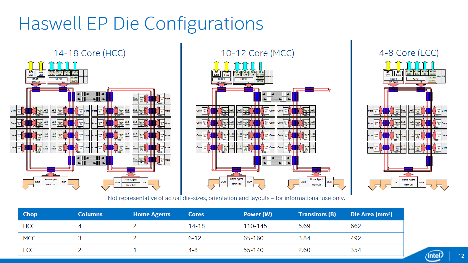
18 Haswell cores, 5.69B transistors and a die area of 662mm², which makes the GTX Titan look small in comparison. A great way to start IDF") .
.
While some sites previously reported that an "unknown source" told them Intel was cooking up a 14-core Haswell EP Xeon chip, and that the next generation 14 nm Xeon E5 "Broadwell" would be an 18-core design, the reality is that Intel has an 18-core Haswell EP design, and we have it for testing. This is yet another example of truth beating fiction.
The Xeon E5-2650L v3 however is the true star of this review. It is power efficient (obviously) and contrary to previous low power offerings it still offers a good response time. Perhaps more surprising is that it even performs well in our FP intensive applications.
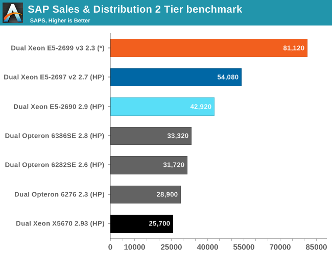
At the other end of the spectrum, the Xeon E5-2699 v3 is much more power hungry than we are used to from a high end part. It shines in SAP where hardware costs are dwarfed by the consulting invoices and delivers maximum performance in HPC. However, the peak power draw of this CPU is nothing to laugh about. Of course, the HPC crowd are used to powerhogs (e.g. GPGPU), but there's a reason Intel doesn't usually offer >130W TDP processors.
Considering the new Haswell EP processors will require a completely new platform motherboards, memory, and processors all need to be upgraded at least initially the parts will mostly be of interest to new server buyers. There are also businesses that demand the absolute fastest servers available and they'll be willing to upgrade, but for many the improvements with Haswell EP may not be sufficient to entice them into upgrading. The 14 nm Broadwell EP will likely be a better time to update servers, but that's still a year or so away.
18 Haswell cores, 5.69B transistors and a die area of 662mm², which makes the GTX Titan look small in comparison. A great way to start IDF
.
