This is a repost of my analysis on why Intel's purported density means NOTHING in discussion of actually implemented density on chips:
Post 1 -
https://www.semiwiki.com/forum/content/6713-14nm-16nm-10nm-7nm-what-we-know-now.html
View attachment 6454
Post 2 -
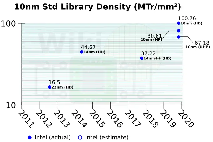
So, I thought at first that the 66MTr/mm2 was from the estimated density for the Apple A12, which was floated around the time of its release. I was wrong. Here is the information to analyze density comparisons for process nodes to put them into context:
This is the list on approximate transistor densities with some information on context. (full source:
https://www.techcenturion.com/7nm-10nm-14nm-fabrication ).
As you can see, when you compare Intel's SRAM numbers, the only one provided, to TSMC's HPC process, that is where the comparing 100.8 to 66.7MTr/mm2 comes from. But take notice that TSMC's low power process for mobile chips is at 96.5MTr/mm2.
Now, let us examine an Anandtech chart looking at actual densities in final silicon:
https://www.anandtech.com/show/13687/qualcomm-snapdragon-8cx-wafer-on-7nm
Notice that for the companies that used the TSMC 7nm FF/FF+ node, Qualcomm reached to up to 94.6MTr/mm2, the HiSilicon Kirin reached 93.1MTr/mm2, and the Apple A12 Bionic reached 82.9MTr/mm2. Those are 98%, 96.5%, and 86%, respectively, of the theorized transistor density. That is pretty good.
But let's examine what happens when we look at Intel's 14nm process, with the theoretical density of 43.5MTr/mm2. Intel, with Skylake 4+2 achieved just 14.3MTr/mm2, or a 33% density compared to the theoretical value that Intel published.
Let's look at AMD's results. Using Samsung/GF 14nm process with a theoretical transistor density off 32.5MTr/mm2, they achieved an actual density of 25MTr/mm2, or 77% of the theorized density. That is pretty good.
So, assuming that the achieved density versus theoretical will be approximately the same, while AMD is using the HPC TSMC process rather than the more dense low power variant, you would take the 66.7MTr/mm2 * 0.77 (77%), which equals 51.3MTr/mm2.
Now it is time for Intel. So, taking the theoretical 100.8MTr/mm2 * 0.33 (33%), you get 33.3MTr/mm2, or roughly 18MTR/mm2 less dense than AMD.
Now, one reason to do less density is heat. By making it less dense, the neighboring transistors contribute less so that the heat density is lower which can allow for higher frequencies at the same temp as a denser chip with lower frequencies. This is part of where Intel gets their high frequency. But, with that, you also wind up with fewer transistors to contribute to doing the work. So, there is a theoretical IPC trade-off. This also isn't comparing the final transistor count nor the die area, although those are provided in the table above. When doing that, you can see why I am very impressed with Intel's engineers ability to design microarchitecture. They have great performance with about 60% of the density of a Ryzen chip, while achieving 25% more frequency, with the rest coming from IPC due to architectural design.
One should always show respect for achievements. AMD deserves respect for achieving the density that they have, Intel on microarchitecture. But to look at densities in a vacuum, especially theorized on SRAM instead of actual results achieved, is more than misleading.