Gideon
Platinum Member
Damn IBM's Telum II architecture looks really interesting:

 www.servethehome.com
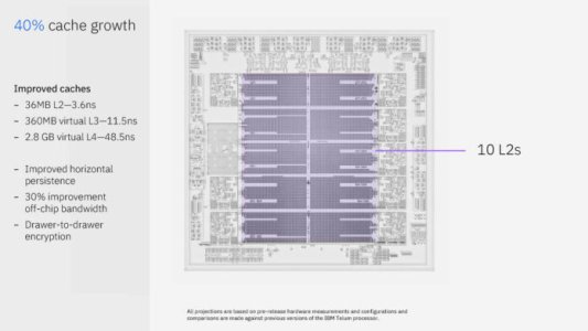
The caches are particularily impressive, especially the the latency considering the size:

I wish we had a gaming-oriented architecture with a similar cache layout. Huge L2 caches can be quite benefitial (looking at Snapdragon X and Apple M series) And on the x86 side we are stuck with 1 - 3MB L2 caches. And the latency for every layer is great.
L4 latency is a bit high but considering it's fetching from a separate chiplet, it's still OK. And if it offers significantly more bandwidth than DRAM it'll still be worth it
More on the Virtual L3 caches from this older Anandtech article:
 www.anandtech.com
But yeah, you win some and lose some. on the Original Telum the virtual L3 bandwidth was quite limited, when the tags were in other L2 slices:
Then again such a massive L2 would also alleviate the pressure somewhat.
This is how the L4 works:
All in all, there's loads of other interesting stuff like the on-die DPU (before the PCIE bus), etc ...

IBM Telum II Processor and Spyre AI Updates at Hot Chips 2024
The new IBM Telum II is the company's next-gen IBM Z mainframe processor with built-in AI and DPU. The company also has a Spyre AI processor
The caches are particularily impressive, especially the the latency considering the size:

I wish we had a gaming-oriented architecture with a similar cache layout. Huge L2 caches can be quite benefitial (looking at Snapdragon X and Apple M series) And on the x86 side we are stuck with 1 - 3MB L2 caches. And the latency for every layer is great.
L4 latency is a bit high but considering it's fetching from a separate chiplet, it's still OK. And if it offers significantly more bandwidth than DRAM it'll still be worth it
More on the Virtual L3 caches from this older Anandtech article:
AnandTech Forums: Technology, Hardware, Software, and Deals
Seeking answers? Join the AnandTech community: where nearly half-a-million members share solutions and discuss the latest tech.
The concept is that the L2 cache isn’t just an L2 cache. On the face of it, each L2 cache is indeed a private cache for each core, and 32 MB is stonkingly huge. But when it comes time for a cache line to be evicted from L2, either purposefully by the processor or due to needing to make room, rather than simply disappearing it tries to find space somewhere else on the chip. If it finds a space in a different core’s L2, it sits there, and gets tagged as an L3 cache line.
What IBM has implemented here is the concept of shared virtual caches that exist inside private physical caches. That means the L2 cache and the L3 cache become the same physical thing, and that the cache can contain a mix of L2 and L3 cache lines as needed from all the different cores depending on the workload. This becomes important for cloud services (yes, IBM offers IBM Z in its cloud) where tenants do not need a full CPU, or for workloads that don’t scale exactly across cores.
This means that the whole chip, with eight private 32 MB L2 caches, could also be considered as having a 256 MB shared ‘virtual’ L3 cache. In this instance, consider the equivalent for the consumer space: AMD’s Zen 3 chiplet has eight cores and 32 MB of L3 cache, and only 512 KB of private L2 cache per core. If it implemented a bigger L2/virtual L3 scheme like IBM, we would end up with 4.5 MB of private L2 cache per core, or 36 MB of shared virtual L3 per chiplet.
But yeah, you win some and lose some. on the Original Telum the virtual L3 bandwidth was quite limited, when the tags were in other L2 slices:
This IBM Z scheme has the lucky advantage that if a core just happens to need data that sits in virtual L3, and that virtual L3 line just happens to be in its private L2, then the latency of 19 cycles is much lower than what a shared physical L3 cache would be (~35-55 cycle). However what is more likely is that the virtual L3 cache line needed is in the L2 cache of a different core, which IBM says incurs an average 12 nanosecond latency across its dual direction ring interconnect, which has a 320 GB/s bandwidth. 12 nanoseconds at 5.2 GHz is ~62 cycles, which is going to be slower than a physical L3 cache, but the larger L2 should mean less pressure on L3 use. But also because the size of L2 and L3 is so flexible and large, depending on the workload, overall latency should be lower and workload scope increased.
Then again such a massive L2 would also alleviate the pressure somewhat.
This is how the L4 works:
But it doesn’t stop there. We have to go deeper.
For IBM Telum, we have two chips in a package, four packages in a unit, four units in a system, for a total of 32 chips and 256 cores. Rather than having that external L4 cache chip, IBM is going a stage further and enabling that each private L2 cache can also house the equivalent of a virtual L4.
This means that if a cache line is evicted from the virtual L3 on one chip, it will go find another chip in the system to live on, and be marked as a virtual L4 cache line.
This means that from a singular core perspective, in a 256 core system, it has access to:
- 32 MB of private L2 cache (19-cycle latency)
- 256 MB of on-chip shared virtual L3 cache (+12ns latency)
- 8192 MB / 8 GB of off-chip shared virtual L4 cache (+? latency)
All in all, there's loads of other interesting stuff like the on-die DPU (before the PCIE bus), etc ...
Last edited:
