
[Ars Technica] IBM and the 7 nm breakthrough
- Thread starter Mondozei
- Start date
You are using an out of date browser. It may not display this or other websites correctly.
You should upgrade or use an alternative browser.
You should upgrade or use an alternative browser.
IBM isn't dead after all.
Usually in the foundry market what counts is lots of production silicon delivered in a timely fashion accompanied of very high yields. This press release is far, far away from that.
IBM is good at...press releases.
They do seem to have some fight left in them though: Power8 vs Xeon E7
NTMBK
Lifer
- Nov 14, 2011
- 10,237
- 5,020
- 136
They do seem to have some fight left in them though: Power8 vs Xeon E7
They are losing in perf/W:
Ultimately, the POWER8 is able to offer slightly higher raw performance than the Intel CPUs, however it just won't be able to do so at the same performance/watt.
sm625
Diamond Member
- May 6, 2011
- 8,172
- 137
- 106
From the article:
What are these guys smoking? Where can I buy a 14nm graphics card? 7nm in two years? Ha! We'll be lucky to see 14nm in two years at this rate. Why are graphics being pooped on so heavily these days? The best video cards produced today cannot even run 4K games at 60fps.
All told, IBM and its partners are targeting "at least a 50 percent power/performance improvement for the next generation of systems"—that is, from 10nm down to 7nm. The difference over 14nm, which is the current state of the art for commercially shipping products, will be even more pronounced.
What are these guys smoking? Where can I buy a 14nm graphics card? 7nm in two years? Ha! We'll be lucky to see 14nm in two years at this rate. Why are graphics being pooped on so heavily these days? The best video cards produced today cannot even run 4K games at 60fps.
NTMBK
Lifer
- Nov 14, 2011
- 10,237
- 5,020
- 136
From the article:
What are these guys smoking? Where can I buy a 14nm graphics card? 7nm in two years? Ha! We'll be lucky to see 14nm in two years at this rate. Why are graphics being pooped on so heavily these days? The best video cards produced today cannot even run 4K games at 60fps.
High end cellphone processors are where the money is these days. Apple has been at 20nm since September last year, Samsung's been shipping a 14nm processor for months.
Fjodor2001
Diamond Member
- Feb 6, 2010
- 3,777
- 247
- 106
From the article:
Regardless, I still think it's cool they they already have test dies on 7 nm. And the more competition we get the better.
Can IBM really manage to roll out 7 nm in 2017/2018? That would be around the same time as Intel/TSMC is expected to provide 10 nm.10 nm is currently being commercialised by Intel, TSMC, GlobalFoundries, and Samsung. It is much too early to guess when 7nm might hit mass production. Earlier this week, a leaked document claimed that Intel was facing difficulties at 10nm and that Cannonlake (due in 2016/2017) had been put on hold. In theory, 7nm should roll around in 2017/2018, but we wouldn't be surprised if it misses that target by some margin.
If IBM and friends actually get 10nm and then 7nm out of the door with relative ease, though, then Intel's process mastery might finally be in contention.
Regardless, I still think it's cool they they already have test dies on 7 nm. And the more competition we get the better.
Fjodor2001
Diamond Member
- Feb 6, 2010
- 3,777
- 247
- 106
Ok, so you're suspecting IBM will "sell" the IP rights to someone else who will make actual products from it? Any chance that "someone else" (Intel/TSMC/Samsung/[...]) will be able to make products based on that in 2017/2018?
IBM has always been a complete bad-ass in the laboratory, and I'm sure they make a boatload off of the 'Intellectual Property' they generate.
But getting it into a shipping product? Not so much.
They do make a lot of money off their IP. Their vast IP resources are always why they are very rarely involved in serious patent disputes or attacked by patent trolls. Basically, anybody involved in tech is probably violating an IBM patent on some level. And they all know it.
shady28
Platinum Member
- Apr 11, 2004
- 2,520
- 397
- 126
Ok, so you're suspecting IBM will "sell" the IP rights to someone else who will make actual products from it? Any chance that "someone else" (Intel/TSMC/Samsung/[...]) will be able to make products based on that in 2017/2018?
IBM has been spitting out patents for decades. In fact, they've been granted more patents every year than any other company for 22 years. They spend > $6 Billion / yr on R&D and take in over $1 Billion / yr in patent licensing.
You can bet that whatever tech they've developed is for sale. They really aren't that interested in manufacturing anymore, it's all about services and IP.
sm625
Diamond Member
- May 6, 2011
- 8,172
- 137
- 106
Yeah but what gets me is that graphics chips are the easiest things to design. They are heterogenous. Their power requirements dont matter all that much. They should be the first on a node. Smartphone SoCs are monstrously complex in comparison. I cant wait for people to stop paying $600 for smartphones. It is such a waste of money and it drags everything else down. I guess what we need is for AMD or Nvidia to start releasing a monster GPU on a two year idiot plan like all the cell carriers do.
SAAA
Senior member
- May 14, 2014
- 541
- 126
- 116
Yeah but what gets me is that graphics chips are the easiest things to design. They are heterogenous. Their power requirements dont matter all that much. They should be the first on a node. Smartphone SoCs are monstrously complex in comparison. I cant wait for people to stop paying $600 for smartphones. It is such a waste of money and it drags everything else down. I guess what we need is for AMD or Nvidia to start releasing a monster GPU on a two year idiot plan like all the cell carriers do.
I'm in.
No for real, where's my 15/month, 2 years plan for a high end video card + monthly games? :sneaky:
WhoBeDaPlaya
Diamond Member
- Sep 15, 2000
- 7,414
- 401
- 126
myocardia
Diamond Member
- Jun 21, 2003
- 9,291
- 30
- 91
Easy to design does not mean easy to fab, though.Yeah but what gets me is that graphics chips are the easiest things to design.
") Small die area means easy to fab, and the SOCs in $600 phones are many times smaller than the GPUs that nVidia and AMD have fabbed.
Small die area means easy to fab, and the SOCs in $600 phones are many times smaller than the GPUs that nVidia and AMD have fabbed.
Last edited:
myocardia
Diamond Member
- Jun 21, 2003
- 9,291
- 30
- 91
We need to get IDC in here since he's a process guy
I know, right? Anyone have the slightest idea what time it is in 台北市?
Phynaz
Lifer
- Mar 13, 2006
- 10,140
- 819
- 126
We need to get IDC in here since he's a process guy
Do you interface with the process teams at all?
I am wondering if I read this correctly:
So they are using EUV which supposedly has long exposure times due to output power problems from the light source through the mask to the wafer, and they are quad-patterning it? Are they using the term "quad-patterning" to mean that they are using four different masks for each layer and then exposing each one? With a 13nm light source why do they need to quad-pattern a 7nm feature size? And how long would that actually take in a real fab? Everyone is moaning about double-patterning using a 193nm light source on 20nm and smaller and the effect on throughput (and thus on cost). I thought one of the wonderful things about EUV was that you could get rid of double-patterning, but if this article is to be believed (and I'm reading it correctly) they are actually taking a much slower lithography patterning machine (EUV) and then using four masks per layer... which seems like it would take so long that it never be commercially viable... and I'm not sure that I understand why you even need to do anything this complex.
Anyway, it's interesting.... it just seems perplexingly complex and extremely far from commercialization in a high volume fab that needs higher wafer throughput to maintain cost effectiveness.
As always, I am not speaking on behalf of my employer, and my opinions are my own.
As background reading, this link talks about the problems of exposure times on EUV:
http://spectrum.ieee.org/semiconductors/devices/euv-chipmaking-inches-forward
and this one talks about the talks about the way node sizes are named - something that IDC has been talking about for years but I only finally understood what he was saying fairly recently - and problems at 14nm and below:
http://spectrum.ieee.org/semiconductors/devices/the-status-of-moores-law-its-complicated
And by the way, while I'm posting up about EUV, I would just like to point out that the way that the light source is made - by dropping molten tin into a high power laser beam which vaporizes the tin and creates 13.5nm ultraviolet light seems completely crazy to me. I understand that this is where the industry is headed, but as a source of light dropping molten metal into a laser beam while you have a jet of hydrogen gas to steer the drops seems completely Rube-Goldbergian to me. It might be practical, it might be necessary, but it still seems like "you have to be kidding me... really? that's the way it works?".
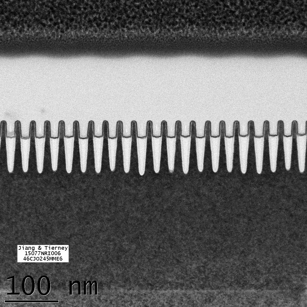
To reach such tiny geometries, self-aligned quadruple patterning (SAQR) and EUV lithography is used.
So they are using EUV which supposedly has long exposure times due to output power problems from the light source through the mask to the wafer, and they are quad-patterning it? Are they using the term "quad-patterning" to mean that they are using four different masks for each layer and then exposing each one? With a 13nm light source why do they need to quad-pattern a 7nm feature size? And how long would that actually take in a real fab? Everyone is moaning about double-patterning using a 193nm light source on 20nm and smaller and the effect on throughput (and thus on cost). I thought one of the wonderful things about EUV was that you could get rid of double-patterning, but if this article is to be believed (and I'm reading it correctly) they are actually taking a much slower lithography patterning machine (EUV) and then using four masks per layer... which seems like it would take so long that it never be commercially viable... and I'm not sure that I understand why you even need to do anything this complex.
Anyway, it's interesting.... it just seems perplexingly complex and extremely far from commercialization in a high volume fab that needs higher wafer throughput to maintain cost effectiveness.
As always, I am not speaking on behalf of my employer, and my opinions are my own.
As background reading, this link talks about the problems of exposure times on EUV:
http://spectrum.ieee.org/semiconductors/devices/euv-chipmaking-inches-forward
and this one talks about the talks about the way node sizes are named - something that IDC has been talking about for years but I only finally understood what he was saying fairly recently - and problems at 14nm and below:
http://spectrum.ieee.org/semiconductors/devices/the-status-of-moores-law-its-complicated
And by the way, while I'm posting up about EUV, I would just like to point out that the way that the light source is made - by dropping molten tin into a high power laser beam which vaporizes the tin and creates 13.5nm ultraviolet light seems completely crazy to me. I understand that this is where the industry is headed, but as a source of light dropping molten metal into a laser beam while you have a jet of hydrogen gas to steer the drops seems completely Rube-Goldbergian to me. It might be practical, it might be necessary, but it still seems like "you have to be kidding me... really? that's the way it works?".
Last edited:
PaulIntellini
Member
- Jun 2, 2015
- 58
- 4
- 71
for a research chip, you only have to find one transistor out of a trillion that works.
for a commercial chip, you have to make sure pretty much every transistor works.
IBM = no SOI anymore ?
for a commercial chip, you have to make sure pretty much every transistor works.
IBM = no SOI anymore ?
Last edited:
shady28
Platinum Member
- Apr 11, 2004
- 2,520
- 397
- 126
Some questions answered here :
http://blog.timesunion.com/business/a-look-at-ibms-new-7nm-chip-wafer-made-in-albany/67677/
http://blog.timesunion.com/business/a-look-at-ibms-new-7nm-chip-wafer-made-in-albany/67677/
IBM teamed with GlobalFoundries and Samsung on the advance. Even though IBM sold off its manufacturing, it is spending $3 billion over five years on chip advances that will be manufactured by GlobalFoundries at its Fab 8 chip factory in Malta. The two companies have a 10-year agreement for GlobalFoundries to make chips for IBMs servers, supercomputers and other semiconductor products.
TRENDING THREADS
-
 Discussion Intel current and future Lakes & Rapids thread
- Started by TheF34RChannel
- Replies: 23K
-
 Discussion Zen 5 Speculation (EPYC Turin and Strix Point/Granite Ridge - Ryzen 9000)
- Started by DisEnchantment
- Replies: 10K
-
 Discussion Speculation: Zen 4 (EPYC 4 "Genoa", Ryzen 7000, etc.)
- Started by Vattila
- Replies: 13K
-
Discussion Intel Meteor, Arrow, Lunar & Panther Lakes Discussion Threads
- Started by Tigerick
- Replies: 7K
-

AnandTech is part of Future plc, an international media group and leading digital publisher. Visit our corporate site.
© Future Publishing Limited Quay House, The Ambury, Bath BA1 1UA. All rights reserved. England and Wales company registration number 2008885.