- Mar 11, 2000
- 23,587
- 1,001
- 126
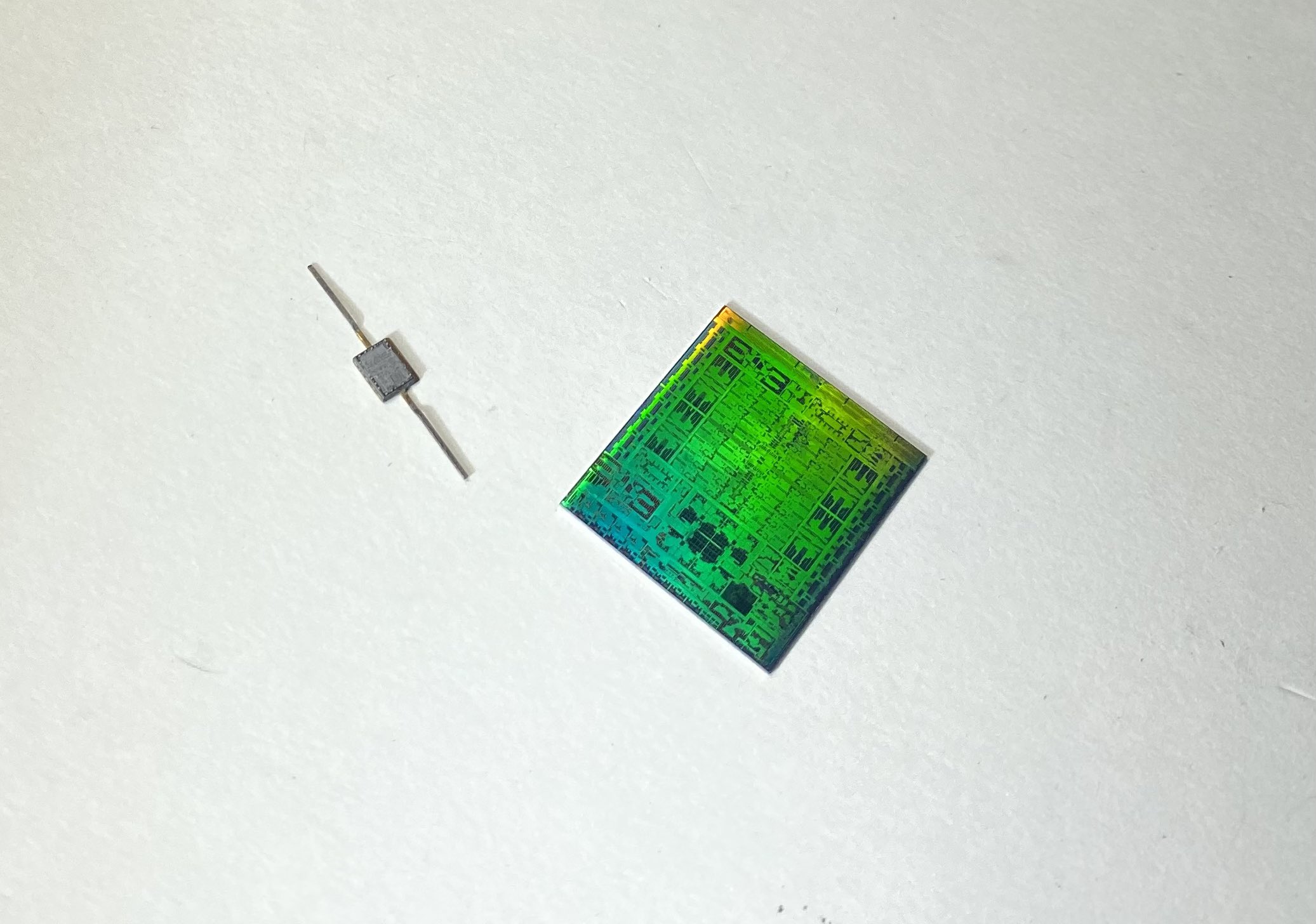
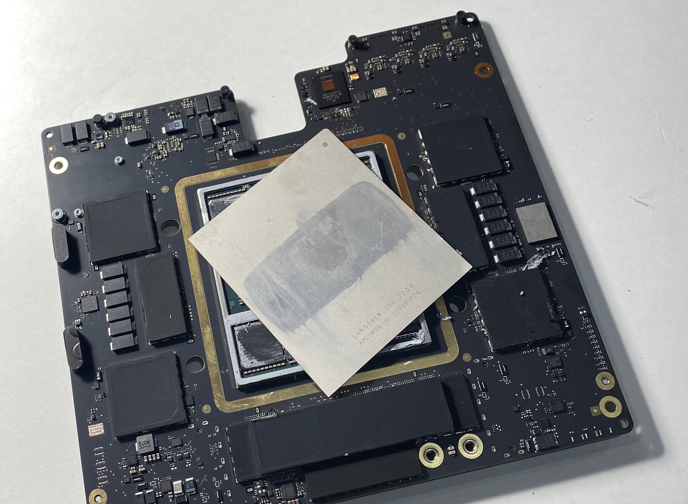
M1
5 nm
Unified memory architecture - LP-DDR4
16 billion transistors
8-core CPU
4 high-performance cores
192 KB instruction cache
128 KB data cache
Shared 12 MB L2 cache
4 high-efficiency cores
128 KB instruction cache
64 KB data cache
Shared 4 MB L2 cache
(Apple claims the 4 high-effiency cores alone perform like a dual-core Intel MacBook Air)
8-core iGPU (but there is a 7-core variant, likely with one inactive core)
128 execution units
Up to 24576 concurrent threads
2.6 Teraflops
82 Gigatexels/s
41 gigapixels/s
16-core neural engine
Secure Enclave
USB 4
Products:
$999 ($899 edu) 13" MacBook Air (fanless) - 18 hour video playback battery life
$699 Mac mini (with fan)
$1299 ($1199 edu) 13" MacBook Pro (with fan) - 20 hour video playback battery life
Memory options 8 GB and 16 GB. No 32 GB option (unless you go Intel).
It should be noted that the M1 chip in these three Macs is the same (aside from GPU core number). Basically, Apple is taking the same approach which these chips as they do the iPhones and iPads. Just one SKU (excluding the X variants), which is the same across all iDevices (aside from maybe slight clock speed differences occasionally).
EDIT:

M1 Pro 8-core CPU (6+2), 14-core GPU
M1 Pro 10-core CPU (8+2), 14-core GPU
M1 Pro 10-core CPU (8+2), 16-core GPU
M1 Max 10-core CPU (8+2), 24-core GPU
M1 Max 10-core CPU (8+2), 32-core GPU
M1 Pro and M1 Max discussion here:
 forums.anandtech.com
M1 Ultra discussion here:
forums.anandtech.com
M2 discussion here:
forums.anandtech.com
Second Generation 5 nm
Unified memory architecture - LPDDR5, up to 24 GB and 100 GB/s
20 billion transistors
8-core CPU
4 high-performance cores
192 KB instruction cache
128 KB data cache
Shared 16 MB L2 cache
4 high-efficiency cores
128 KB instruction cache
64 KB data cache
Shared 4 MB L2 cache
10-core iGPU (but there is an 8-core variant)
3.6 Teraflops
16-core neural engine
Secure Enclave
USB 4
Hardware acceleration for 8K h.264, h.264, ProRes
M3 Family discussion here:
forums.anandtech.com
5 nm
Unified memory architecture - LP-DDR4
16 billion transistors
8-core CPU
4 high-performance cores
192 KB instruction cache
128 KB data cache
Shared 12 MB L2 cache
4 high-efficiency cores
128 KB instruction cache
64 KB data cache
Shared 4 MB L2 cache
(Apple claims the 4 high-effiency cores alone perform like a dual-core Intel MacBook Air)
8-core iGPU (but there is a 7-core variant, likely with one inactive core)
128 execution units
Up to 24576 concurrent threads
2.6 Teraflops
82 Gigatexels/s
41 gigapixels/s
16-core neural engine
Secure Enclave
USB 4
Products:
$999 ($899 edu) 13" MacBook Air (fanless) - 18 hour video playback battery life
$699 Mac mini (with fan)
$1299 ($1199 edu) 13" MacBook Pro (with fan) - 20 hour video playback battery life
Memory options 8 GB and 16 GB. No 32 GB option (unless you go Intel).
It should be noted that the M1 chip in these three Macs is the same (aside from GPU core number). Basically, Apple is taking the same approach which these chips as they do the iPhones and iPads. Just one SKU (excluding the X variants), which is the same across all iDevices (aside from maybe slight clock speed differences occasionally).
EDIT:
M1 Pro 8-core CPU (6+2), 14-core GPU
M1 Pro 10-core CPU (8+2), 14-core GPU
M1 Pro 10-core CPU (8+2), 16-core GPU
M1 Max 10-core CPU (8+2), 24-core GPU
M1 Max 10-core CPU (8+2), 32-core GPU
M1 Pro and M1 Max discussion here:
Page 78 - Discussion - Apple Silicon SoC thread
Page 78 - Seeking answers? Join the AnandTech community: where nearly half-a-million members share solutions and discuss the latest tech.
M1 Ultra discussion here:
Page 109 - Discussion - Apple Silicon SoC thread
Page 109 - Seeking answers? Join the AnandTech community: where nearly half-a-million members share solutions and discuss the latest tech.
M2 discussion here:
Page 127 - Discussion - Apple Silicon SoC thread
Page 127 - Seeking answers? Join the AnandTech community: where nearly half-a-million members share solutions and discuss the latest tech.
Second Generation 5 nm
Unified memory architecture - LPDDR5, up to 24 GB and 100 GB/s
20 billion transistors
8-core CPU
4 high-performance cores
192 KB instruction cache
128 KB data cache
Shared 16 MB L2 cache
4 high-efficiency cores
128 KB instruction cache
64 KB data cache
Shared 4 MB L2 cache
10-core iGPU (but there is an 8-core variant)
3.6 Teraflops
16-core neural engine
Secure Enclave
USB 4
Hardware acceleration for 8K h.264, h.264, ProRes
M3 Family discussion here:
Page 215 - Discussion - Apple Silicon SoC thread
Page 215 - Seeking answers? Join the AnandTech community: where nearly half-a-million members share solutions and discuss the latest tech.
Last edited: