Looks like N3(E?) will also play a role in Zen5, so the N4 rumors were off. I could go off about a "generic" N3 compute chiplet + N4 IOD, but we all already know Zen5 will be a big redesign (bigger than Zen1 -> Zen2 possibly), so it's useless to speculate much right now. Conventional Zen wisdom may not apply to Zen5 at all. Hell, from the AMD FD slides it looks like RDNA3
might use stacking, few people expected it.
LPDDR5X is 7500-8533MTs, if 8533MTs is too exotic/expensive 10 months from now, maybe 7500MTs is a more realistic "compromise"?
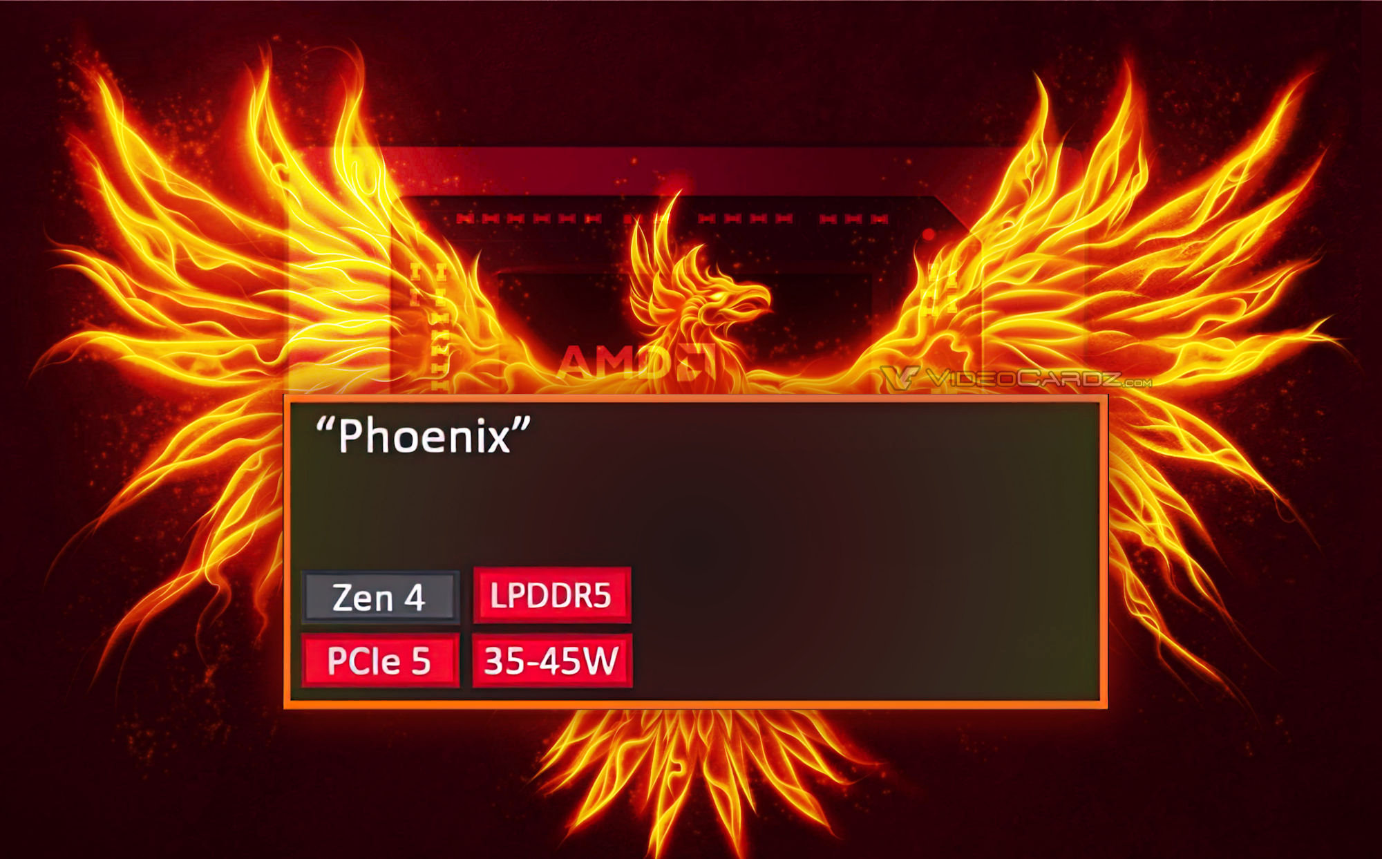
AMD Phoenix APU with mid-range discrete GPU performance Greymon55 claims that the upcoming integrated graphics into the AMD Phoenix APU, could show comparable performance to the most power-restricted version of the RTX 3060 mobile. AMD Ryzen 7000 series will officially include two mobile series...

videocardz.com
Far fetched maybe (2,5x improvement vs typical Radeon 680M iGPU performance), but I do see a scenario where this is very plausible.
One were you pit a 60W 3060M + whatever the CPU it's paired with uses in gaming benchmarks (85W total?) VERSUS top Phoenix Point SKU running at above it's rumored 35W TDP, or roughly the same ~85W TDP as the 60W+CPU 3060M system.
Radeon 680M already needs north of 30W for itself alone to hit and stay at it's rated 2,2/2,4GHz clocks. It's likely RDNA3 iGPUs will also need a somewhat generous power budget to hit and keep the reported 3GHz clocks in game.