
AMD announces 7nm MI60 and MI50 DL accelerators
- Thread starter tamz_msc
- Start date
You are using an out of date browser. It may not display this or other websites correctly.
You should upgrade or use an alternative browser.
You should upgrade or use an alternative browser.
Stuka87
Diamond Member
- Dec 10, 2010
- 6,240
- 2,559
- 136
Quite the informative post there....
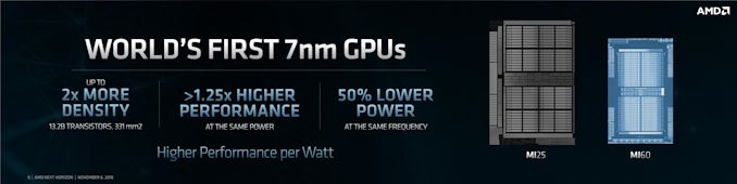
To add a bit of content to this topic. These are 7nm Vega20 based GPUs. But they have the same number of stream processors and such as current Vega chips. Just smaller, so hopefully less power, although clocks are higher at 1800Mhz.
To add a bit of content to this topic. These are 7nm Vega20 based GPUs. But they have the same number of stream processors and such as current Vega chips. Just smaller, so hopefully less power, although clocks are higher at 1800Mhz.
- Jan 5, 2017
- 3,772
- 3,590
- 136
TDP is 300W though.Quite the informative post there....
To add a bit of content to this topic. These are 7nm Vega20 based GPUs. But they have the same number of stream processors and such as current Vega chips. Just smaller, so hopefully less power, although clocks are higher at 1800Mhz.
itsmydamnation
Platinum Member
- Feb 6, 2011
- 2,764
- 3,131
- 136
volta is huge, this is not. its an interesting product, lots of I/O and memory , high FP64 and maybe all the way down to int 1 (someone said they heard that) but atleast int4. Its not world beating but in a way its very rv770 like compared to the competition. The devil will be in the software, if ROCm2 is up to scratch it could be a very good product for amd to get a foothold in a market they haven't really been able to so far.Not really that impressive at 7nm, Volta is still superior even though it is 12nm! And with the same power consumption!

Seems like they're trading power reduction for frequency gains in order to reach the given clock-speeds. Density improvement isn't that great either(comparing 484 mm^2 Vega 10 vs 330 mm^2 Vega 20).
Vega 10 at 1.5ghz is like a ~200watt card (atleast in gaming/crypto). its 1600mhz + it gets stupid.
Volta is 12nm, Vega 20 is freaking 7nm. Volta @7nm will stomp all over it in style, especially when you ramp it's clocks up!volta is huge, this is not.
Stuka87
Diamond Member
- Dec 10, 2010
- 6,240
- 2,559
- 136
Volta is 12nm, Vega 20 is freaking 7nm. Volta @7nm will stomp all over it in style, especially when you ramp it's clocks up!
When he says Huge he means its a larger chip, as in number of transistors.Volta literally has almost twice as many transistors (21B vs 12.5B). And it has a 300W TDP, just like Vega20. Volta has 6.9TF FP64, Vega20 has 7.2TF FP64. Not sure what you are basing this "stomp all over it" phrase on. The two cards are fairly evenly matched when it comes to DL usage.
It means it has headroom to grow on 7nm. With lower power consumption too. Also power efficiency is massive with volta, it can run double the number of transistors at lower energy consumption.And it has tensor cores which highly elevates it above MI60.When he says Huge he means its a larger chip, as in number of transistors.Volta literally has almost twice as many transistors (21B vs 12.5B)
Nope, volta pcie is 250w.And it has a 300W TDP,
Last edited:
Glo.
Diamond Member
- Apr 25, 2015
- 5,705
- 4,549
- 136
300W is the maximum power, designed. Previous MI GPUs have had dual 8 pin connector, for power delivery. MI60 has 6+8 pin power delivery. It will use less power than 300W.I
Nope, volta pcie is 250w.
And yes, the GPU is much better than everybody thought it was going to be.
to you maybe. but compared to the competition, they are still several steps behind even on 7nm vs 12nm300W is the maximum power, designed. Previous MI GPUs have had dual 8 pin connector, for power delivery. MI60 has 6+8 pin power delivery. It will use less power than 300W.
Last edited:
300W is the maximum power, designed. Previous MI GPUs have had dual 8 pin connector, for power delivery. MI60 has 6+8 pin power delivery. It will use less power than 300W.
And yes, the GPU is much better than everybody thought it was going to be.
That is not true at all.
Alot of people were jumping on the 20tflop bandwagon from WCCFtech a while back.
Some people at overclock.net were claiming 44 billion transistors, 30tflop cards based on 2.8 increase in transistor density.
Heck, even AMD slides which initially stated 1.35x performance at the same power have shrunk down to 1.25x performance at the same power.
At a 1.25 increase in tflop count only, this card will be slower than a gtx 1080 ti in gaming considering the bottlenecks of the Vega architecture at higher frequencies and would thus lose to a rtx 2080 which got slammed for it's performance not that long ago.
With only this much tflops, it makes absolute zero sense for AMD to release this as a consumer gaming card which many people wanted. You would be looking at speeds at best 20% faster than vega 64 which put it slight faster than an rtx 2070 but much more difficulty being able price near that region because of the 7nm die and the 4 stacks of HBM2.
This is a new node and you think 25% better than what peoples were expecting considering Nvidia was crapped on for only a 40% performance jump with essentially the same node and was crapped on. Why do people rewrite history, so we can prop one company up and tear another down. It creates a more hostile forum environment because it turns things into videocard politics. Don't lie to yourself. Using the same power while getting 25% more performance is at the bottom tier of peoples expectations considering the move to the new node.
Just to illustrate this further, people said, the rtx 2080 was a disappointing jump with a 40% performance jump from the rtx 1080 to 2080 because the gtx 980 to 1080 was a 66% jump. They call it turding after it was launched because of this disappointing performance jump. So now 25% performance jump on a new node is better than what people were expecting?
Stuka87
Diamond Member
- Dec 10, 2010
- 6,240
- 2,559
- 136
It means it has headroom to grow on 7nm. With lower power consumption too. Also power efficiency is massive with volta, it can run double the number of transistors at lower energy consumption.And it has tensor cores which highly elevates it above MI60.
Nope, volta pcie is 250w.
nVidia's own documentation says Volta cards have a 300W TDP. And I still am not sure where you are getting your information on what a Volta die shrink would bring. Tensor cores use case is pretty narrow. They are very fast for very specific types of calculations, but any other type of calculation won't even use them.
nVidia's own documentation says Volta cards have a 300W TDP. And I still am not sure where you are getting your information on what a Volta die shrink would bring. Tensor cores use case is pretty narrow. They are very fast for very specific types of calculations, but any other type of calculation won't even use them.
The Mezzanine version is 300 W; the pcie version is 250 W.
No, NVIDIA's own data says 250w for the PCIE.nVidia's own documentation says Volta cards have a 300W TDP
https://www.nvidia.com/en-us/data-center/tesla-v100/
Not narrow, they are wide spread within CUDA.Tensor cores use case is pretty narrow.
Volta is already faster than MI25 (with tensor cores), imagine what a 7nm volta would do.And I still am not sure where you are getting your information on what a Volta die shrink would bring.
TDP is 300W though.
The Radeon Instinct MI25 (Vega 10) is also a 300W card, but it has peak clocks of only 1500 MHz. If the MI60 (Vega 20) can do 1800 MHz at the same TDP on essentially the same architecture, that's a pretty healthy gain from TSMC 7nm over GloFo 14nm. 20% clock speed improvement at the same power draw is nothing to sneeze at.
tviceman
Diamond Member
So the MI60 is 25% faster than OG Vega at the same power draw - which puts it right at GTX 2070 performance but using 100 more watts. The die size is much improved, but AMD is still so far behind in efficiency. It seems to me that Vega 20 is a proper shrink of Vega but is otherwise stuck in an old design that didn't extract any performance gains from architectural improvements.
Hopefully Navi can bring actual architectural efficiency improvements, otherwise AMD on 7nm will still be behind Nvidia's half-baked 12nm chips in performance and perf/w.
Hopefully Navi can bring actual architectural efficiency improvements, otherwise AMD on 7nm will still be behind Nvidia's half-baked 12nm chips in performance and perf/w.
So the MI60 is 25% faster than OG Vega at the same power draw - which puts it right at GTX 2070 performance but using 100 more watts. The die size is much improved, but AMD is still so far behind in efficiency. It seems to me that Vega 20 is a proper shrink of Vega but is otherwise stuck in an old design that didn't extract any performance gains from architectural improvements.
Hopefully Navi can bring actual architectural efficiency improvements, otherwise AMD on 7nm will still be behind Nvidia's half-baked 12nm chips in performance and perf/w.
Well, I'm not sure what anyone really expected? However, Fury->Vega was both a die shrink and an architectural change and had a 25% uplift in performance while improving perf/watt by only 6% (according to TPU). So, assuming that Vega 20 is a "simple" die-shrink with no real architectural improvements, this isn't that bad.
I'm not sure either. Given the time scales, likely R&D budget and their starting point they've probably done a decent enough job of making it into a compute card.
It is still likely to end up in a nasty place when Volta's successor rolls up but a huge & growing market so pie for all")
The software stuff they talked about working really well is probably more important in the medium /long term anyway.
It is still likely to end up in a nasty place when Volta's successor rolls up but a huge & growing market so pie for all
The software stuff they talked about working really well is probably more important in the medium /long term anyway.
TRENDING THREADS
-
 Discussion Intel current and future Lakes & Rapids thread
- Started by TheF34RChannel
- Replies: 23K
-
 Discussion Zen 5 Speculation (EPYC Turin and Strix Point/Granite Ridge - Ryzen 9000)
- Started by DisEnchantment
- Replies: 9K
-

-
Discussion Intel Meteor, Arrow, Lunar & Panther Lakes Discussion Threads
- Started by Tigerick
- Replies: 7K
-

AnandTech is part of Future plc, an international media group and leading digital publisher. Visit our corporate site.
© Future Publishing Limited Quay House, The Ambury, Bath BA1 1UA. All rights reserved. England and Wales company registration number 2008885.