- May 11, 2008
- 19,494
- 1,163
- 126
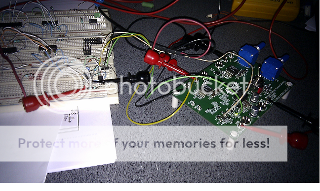
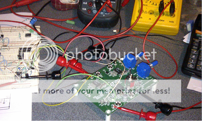
The DC2132A is a very nice powersupply with specs 0-24V and 0 to 3A. And the nice part is that it does not require any heatsinks. It has a step down smps that pre-regulates the voltage down to Voutput + 1,7V. And behind the smps is a linear regulated output stage (comprised of a dual LT3081 setup) to remove any ripple to get a clean output voltage. Added features are thermal monitoring and current monitoring, courtesy of the LT3081.
The LT3081 is used in a dual setup to allow a maximum current of 3A.
Oh well, how the circuit works, a LTspice model is available as is a demoboard, which i am so lucky to posses.") Was sort of needed for work shortly and after it was no longer needed, i could have it. ^_^.
Was sort of needed for work shortly and after it was no longer needed, i could have it. ^_^.
http://www.linear.com/solutions/5086
LT journal with explanation.
http://www.linear.com/docs/45093
As i played with it at home, i found out a worrying fact, when the current control is turned to zero, the output would give of a negative voltage. -0.76V to be exact.
Parasitic diodes.
The problem is that most integrated circuits do not handle negative voltages on their powersupply pins. This is because how ic are build up, by silicon and P and N layers. All ic's have some form of parasitic diodes and parasitic thyristors because of the way the silicon is doped . Usually, we never notice because we apply the correct voltages. and in all datasheets the absolute ratings of supply voltages are given. For example -0.3V to 6V.
https://en.wikipedia.org/wiki/Parasitic_structure
Solution :
So, i had to find a way to solve this. The whole point is that the LT3081 needs a load current with a maximum of 5mA to function. But how are you going to let this current flow if the output is 0V with respect to ground level. Well, a negative powersupply of -5V is used. This -5V is created with another smps. Since it is a regulated voltage, all that is needed is a resistor R2 and a transistor Q1. It might just be that this is the case with my pcb or that it is systematic, anyway this way the bench powersupply is useless. And the problem is because the R2 and Q1 are a static circuit. If there is any tolerance, this circuit will not work. At least, not with my pcb.
My first attempt was to replace R2 with a 470Ohm resistor and a 500 Ohm potentiometer. But when i calibrated the output to 0V, i noticed something problematic. When i quickly turned the voltage potentiometer up and down again, the output voltage would start to float at around 9V. Even while the set input of the LT3081 is at 0V. Only when i turned the voltage potentio meter slowly, would the LT3081 output follow the voltage at the set input.
This was useless and unacceptable and had to think of something else.
Since i am going to use a 10 turn potentiometer for voltage and current control anyway, this might not be an issue but i want to be able to trust my bench power supply.
So, i removed R2 and Q1 and made a circuit with an LM358 (temporary solution, i am going to use another) opamp as an integrator, a transistor with emitter resistor to sink the 2x 5mA(maximum for 2x LT3081) current dynamically instead of statically. I will make a schematic later and post it. But anyway, the inverting input i connected to ground through a 10K resistor and the non inverting input through a 10k resistor to the output. And added a diode at the non inverting terminal of the LM358, so that the maximum common mode voltage of the opamp is never exceeded(output can be 24V). The non inverting input will never come higher then 0.6V with respect to ground this way.
The opamp will try to keep the output at exactly 0V. But it can only sink about 10mA. That is no match for the LT3081 combination that sources a maximum of 3A. But when the output voltage is reduced to zero and the current control is reduced to zero, the opamp circuit i made comes in effect, keeping the load current through the LT3081 combination flowing at a value to make sure that the output voltage is then 0V. And that the load current is high enough that the two LT3081 acutally see a load current since they need this current to function properly.
In the LT journal it is all explained how the circuit works. I will post a schematic later on about the opamp circuit i added.
Why i do this ?
The plan is to add a PIC16LF1509 to read out the voltages that represent the output current and the output voltage. also, because the current is available as a voltage and i always like to have a current trip feature next to a current source mode feature. When i set the current potentiometer to maximum and i set the pic in current trip mode with an extra potentiometer, i can set the trip current where the bench supply will be turned off by the pic.
A fuse mode. To protect expensive ic's in expensive proto circuits.
The pic will be connected to a 2x16 character LCD and a 2 buttons will be added. One for menu, and one to turn the powersupply output on and off.
And the pic will do thermal monitoring. When the temperature outputs of the LT3081(can be put in parallel since they are high impedance current sources) give a high enough voltage over an external resistor, for example the LT3081 has reached 100C, the pic will display "temperature over limit" and turn of the bench supply to protect the LT3081 from overheating.
I will then have a very luxurious bench power supply in a small case.
Schematic :

I do find it sad, that the evaluationboard of Linear Technology is a bit expensive. But the design files and the schematics are available to build one yourself.
I will post a schematic tomorrow about the current sink i created to get the output to a proper 0V.
LT3081 datasheet :
http://www.linear.com/docs/43256
The LT3081 is used in a dual setup to allow a maximum current of 3A.
Oh well, how the circuit works, a LTspice model is available as is a demoboard, which i am so lucky to posses.
Was sort of needed for work shortly and after it was no longer needed, i could have it. ^_^.http://www.linear.com/solutions/5086
LT journal with explanation.
http://www.linear.com/docs/45093
As i played with it at home, i found out a worrying fact, when the current control is turned to zero, the output would give of a negative voltage. -0.76V to be exact.
Parasitic diodes.
The problem is that most integrated circuits do not handle negative voltages on their powersupply pins. This is because how ic are build up, by silicon and P and N layers. All ic's have some form of parasitic diodes and parasitic thyristors because of the way the silicon is doped . Usually, we never notice because we apply the correct voltages. and in all datasheets the absolute ratings of supply voltages are given. For example -0.3V to 6V.
https://en.wikipedia.org/wiki/Parasitic_structure
Solution :
So, i had to find a way to solve this. The whole point is that the LT3081 needs a load current with a maximum of 5mA to function. But how are you going to let this current flow if the output is 0V with respect to ground level. Well, a negative powersupply of -5V is used. This -5V is created with another smps. Since it is a regulated voltage, all that is needed is a resistor R2 and a transistor Q1. It might just be that this is the case with my pcb or that it is systematic, anyway this way the bench powersupply is useless. And the problem is because the R2 and Q1 are a static circuit. If there is any tolerance, this circuit will not work. At least, not with my pcb.
My first attempt was to replace R2 with a 470Ohm resistor and a 500 Ohm potentiometer. But when i calibrated the output to 0V, i noticed something problematic. When i quickly turned the voltage potentiometer up and down again, the output voltage would start to float at around 9V. Even while the set input of the LT3081 is at 0V. Only when i turned the voltage potentio meter slowly, would the LT3081 output follow the voltage at the set input.
This was useless and unacceptable and had to think of something else.
Since i am going to use a 10 turn potentiometer for voltage and current control anyway, this might not be an issue but i want to be able to trust my bench power supply.
So, i removed R2 and Q1 and made a circuit with an LM358 (temporary solution, i am going to use another) opamp as an integrator, a transistor with emitter resistor to sink the 2x 5mA(maximum for 2x LT3081) current dynamically instead of statically. I will make a schematic later and post it. But anyway, the inverting input i connected to ground through a 10K resistor and the non inverting input through a 10k resistor to the output. And added a diode at the non inverting terminal of the LM358, so that the maximum common mode voltage of the opamp is never exceeded(output can be 24V). The non inverting input will never come higher then 0.6V with respect to ground this way.
The opamp will try to keep the output at exactly 0V. But it can only sink about 10mA. That is no match for the LT3081 combination that sources a maximum of 3A. But when the output voltage is reduced to zero and the current control is reduced to zero, the opamp circuit i made comes in effect, keeping the load current through the LT3081 combination flowing at a value to make sure that the output voltage is then 0V. And that the load current is high enough that the two LT3081 acutally see a load current since they need this current to function properly.
In the LT journal it is all explained how the circuit works. I will post a schematic later on about the opamp circuit i added.
Why i do this ?
The plan is to add a PIC16LF1509 to read out the voltages that represent the output current and the output voltage. also, because the current is available as a voltage and i always like to have a current trip feature next to a current source mode feature. When i set the current potentiometer to maximum and i set the pic in current trip mode with an extra potentiometer, i can set the trip current where the bench supply will be turned off by the pic.
A fuse mode. To protect expensive ic's in expensive proto circuits.
The pic will be connected to a 2x16 character LCD and a 2 buttons will be added. One for menu, and one to turn the powersupply output on and off.
And the pic will do thermal monitoring. When the temperature outputs of the LT3081(can be put in parallel since they are high impedance current sources) give a high enough voltage over an external resistor, for example the LT3081 has reached 100C, the pic will display "temperature over limit" and turn of the bench supply to protect the LT3081 from overheating.
I will then have a very luxurious bench power supply in a small case.
Schematic :
I do find it sad, that the evaluationboard of Linear Technology is a bit expensive. But the design files and the schematics are available to build one yourself.
I will post a schematic tomorrow about the current sink i created to get the output to a proper 0V.
LT3081 datasheet :
http://www.linear.com/docs/43256
Last edited: