Info 64MB V-Cache on 5XXX Zen3 Average +15% in Games

Page 3 - Seeking answers? Join the AnandTech community: where nearly half-a-million members share solutions and discuss the latest tech.

Kedas

Senior member
Dec 6, 2018
355
339
136
Well we know now how they will bridge the long wait to Zen4 on AM5 Q4 2022.
Production start for V-cache is end this year so too early for Zen4 so this is certainly coming to AM4.
+15% Lisa said is "like an entire architectural generation"
 
Last edited:
  • Like
Reactions: Tlh97 and Gideon
Jul 27, 2020
16,279
10,316
106
Because Logic transistors such as ALUs, FPUs, branch predictors, decoders use a lot of power per transistor while caches are very power efficient. Power is pretty much the biggest limiter to performance nowadays.

Bit off topic but how come CPU designers haven't thought of using persistent cache for storing decoded instructions? Something connected directly to the CPU with lowest possible latency so the CPU decoders don't have to work as hard? Wouldn't that save a lot of CPU time and increase instruction throughput? Most consumer workloads are just repetitive in nature. Boot PC, load OS, launch frequently used software, use frequently used functions of said software.
 

Makaveli

Diamond Member
Feb 8, 2002
4,718
1,054
136
Any link please? All the Alder Lake engineering sample performance leaks show worse latency. At least the ones that I've seen.


This is your Alderlake sample here


And this is the text below the numbers

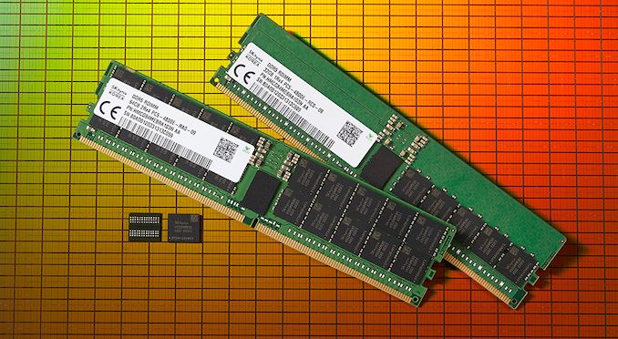
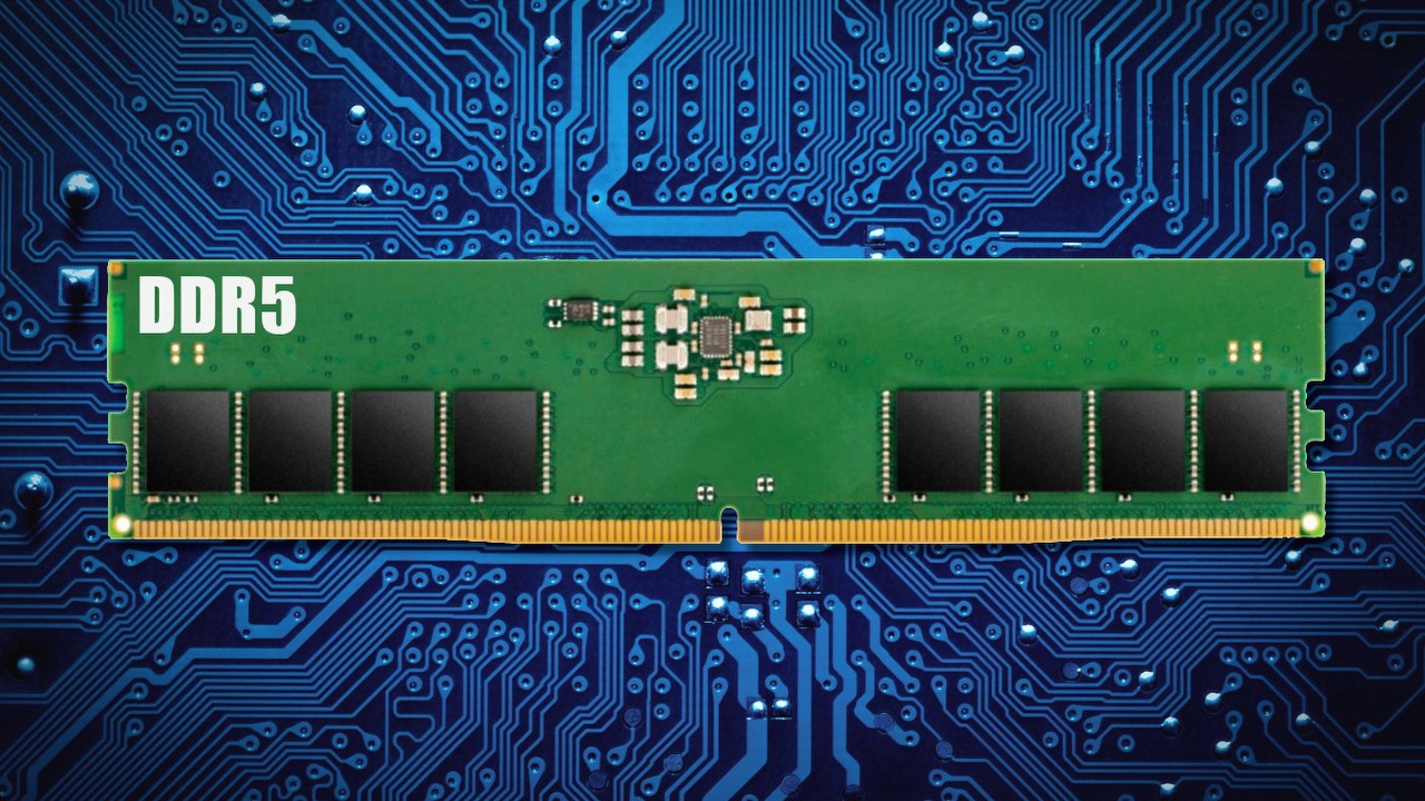
CL40 latency (40-40-40-77) may raise some concern, but it's worth remembering that this is only the number of cycles needed to receive data from a memory cell. Better bandwidth requires higher clock speeds for RAM chips - but at the same time, the time per cycle decreases. That's why, despite increasing CL values in successive generations of DDR memory, the access latency actually remains at a similar level.
 
Last edited:
  • Like
Reactions: Elfear

IntelUser2000

Elite Member
Oct 14, 2003
8,686
3,785
136
By the way another reason V-cache is faster than Intel's eDRAM is because SRAM is faster than DRAM.

Bit off topic but how come CPU designers haven't thought of using persistent cache for storing decoded instructions?

What do you mean by a persistent cache? Persistent as in no data lost when power is off?

There's no technology that's fast enough to be used in CPUs while being non-volatile. Unless you mean something else.
 

JoeRambo

Golden Member
Jun 13, 2013
1,814
2,105
136
And why would V-cache not require tags? I assume the stacks will have tags in them. It sounds like it's just an extension of the existing L3.

Of course they will have tags, but in case of EDRAM L4, tags were on BDW chip, replacing actual L3 to save on latency. Otherwise you have to go to actual L4 cache each time ( might as well convert it to system side cache and call it a day at that point ). AMDs solution is simply more of good old L3 cache, they don't even need to replicate L2 shadow tags in the chip as that is already handled by L3 cache complex in original CCD, just SRAM for actual L3 lines and tags with whatever redundancy they need to achieve almost 100% yield.
 

IntelUser2000

Elite Member
Oct 14, 2003
8,686
3,785
136
Of course they will have tags, but in case of EDRAM L4, tags were on BDW chip, replacing actual L3 to save on latency.

Yes, I hadn't thought of that. Good point!

They changed that with Skylake. I wonder how much performance impact was there by changing the system? I thought the poor performance of the GT4e version might have had to do with that.
 

Hougy

Member
Jan 13, 2021
77
60
61
I know what you mean.

The Square root law in microprocessors say that if you increase the number of transistors by X%, the actual performance you get is square root of X. So if you quadruple the number of transistors, you get twice the performance. It's not just die area that's quadrupled. The power use is quadrupled as well, since 4x the transistors.

You can use clever engineering and ideas to overcome that somewhat but new ideas are much harder to come by.

Intel's Cypress Cove(the 14nm version of Icelake's core) uses 37% more transistors for 18% performance. Follows the law almost exactly. :)

But this is a generalized statement. Because Logic transistors such as ALUs, FPUs, branch predictors, decoders use a lot of power per transistor while caches are very power efficient. Power is pretty much the biggest limiter to performance nowadays.

Caches, and the way AMD does it will add die area and cost, but is a very power efficient way to increase performance.
Thanks again for the informative reply.

What I was thinking initially is that instead of using 36mm^2 of silicon (44,4% more) in cache and get 15% more performance, they could use it in a mixture of logic and cache to get 20% more performance according to the square root law. But that approach would probably incur in many more additional costs since the Zen 3 die would have to be remade.

If I understood correctly, you're saying now is that because cache uses less power, X% more cache could result in more than sqrt(X) of performance increase. That was not the case here. Looks like the Zen 3 cores are not in a huge need of more cache.
 

IntelUser2000

Elite Member
Oct 14, 2003
8,686
3,785
136
If I understood correctly, you're saying now is that because cache uses less power, X% more cache could result in more than sqrt(X) of performance increase. That was not the case here. Looks like the Zen 3 cores are not in a huge need of more cache.

In terms of power use, it'll add something like less than 5% on the desktop chips. And you'll definitely get 5%+ performance gains in average(that's what we got with Broadwell!), and scenarios like games and other applications where it has a larger dataset, 10-20%, which is absolutely huge.

Nevermind the square root law. That's superlinear scaling!
 
Jul 27, 2020
16,279
10,316
106
This is your Alderlake sample here


I'm confused. Isn't that link showing 97% increased latency? Elsewhere on the internet, I've read comments that DDR5's latency will be on par with DDR4's only past 8000 MT/s.
 

maddie

Diamond Member
Jul 18, 2010
4,740
4,674
136
Curious here. Anyone has an idea of the memory size needed for storing say, 90% of most used X86 instructions converted to uops?
 

maddie

Diamond Member
Jul 18, 2010
4,740
4,674
136
I'm confused. Isn't that link showing 97% increased latency? Elsewhere on the internet, I've read comments that DDR5's latency will be on par with DDR4's only past 8000 MT/s.
It's in the linked article.

CL - CAS Latency

CL40 latency (40-40-40-77) may raise some concern, but it's worth remembering that this is only the number of cycles needed to receive data from a memory cell. Better bandwidth requires higher clock speeds for RAM chips - but at the same time, the time per cycle decreases. That's why, despite increasing CL values in successive generations of DDR memory, the access latency actually remains at a similar level.
 
Jul 27, 2020
16,279
10,316
106
That's why, despite increasing CL values in successive generations of DDR memory, the access latency actually remains at a similar level.

The reduction in latency is particularly impressive when you jump up to DDR3-1600, it only takes 33.5ns to access main memory.

To show the memory latency of the Rocket Lake CPU, the Chiphell user first tested a DDR4-4000 kit with 18-20-20-40 1T timings. The 1:1 threshold led to 61.3 nanosecond latencies in AIDA64 and with a DDR4-3600 14-14-14-34 2T kit with uncore clocks set to 4,100 MHz and got 50.2 ns latency.

Nehalem running DDR3-1600 needed 33.5ns to access main memory.
Rocket Lake running DDR4-3600 needs 50.2ns

Maybe I'm misunderstanding something? Yes, Rocket Lake fetches tons more data than Nehalem in a given time period but actual RAM access latency has increased, no? DDR5's leaked benchmarks are showing that it will go over 100ns. How is that better?
 
Jul 27, 2020
16,279
10,316
106
Curious here. Anyone has an idea of the memory size needed for storing say, 90% of most used X86 instructions converted to uops?
Due to the sheer amount of instructions CPUs can process per second, this is likely going to be in gigabytes. For the average PC user, it could be much less if they cycle between just a few frequently used applications/games.


You have this expensive logic block chunking away. Now we just stuff those micro-ops into the op-cache, all the decoding done, and the hit-rate there is really high [Clark: up to 90% on a lot of workloads], so that means we’re only doing that heavy-weight decode 10% of the time.

AMD is doing this on-chip, just not in a persistent non-volatile manner. This seems to suggest that the opcache size might be in megabytes at most.
 

maddie

Diamond Member
Jul 18, 2010
4,740
4,674
136


Nehalem running DDR3-1600 needed 33.5ns to access main memory.
Rocket Lake running DDR4-3600 needs 50.2ns

Maybe I'm misunderstanding something? Yes, Rocket Lake fetches tons more data than Nehalem in a given time period but actual RAM access latency has increased, no? DDR5's leaked benchmarks are showing that it will go over 100ns. How is that better?
Check out the table on this page for the actual ram module latencies.

DDR3 1600 : 13.75 ns - 7.5 ns CAS 11 - 6
DDR4 3600 : 10.56 ns - 8.33 ns CAS 19 - 15


maddie

Diamond Member
Jul 18, 2010
4,740
4,674
136
Due to the sheer amount of instructions CPUs can process per second, this is likely going to be in gigabytes. For the average PC user, it could be much less if they cycle between just a few frequently used applications/games.


AMD is doing this on-chip, just not in a persistent non-volatile manner. This seems to suggest that the opcache size might be in megabytes at most.
I think I asked this question incorrectly. The present micro ops cache is only a few KB in size. All I wanted was how big it would be for most of X86 instructions.

As an example Haswell was ~ 4 B/micro-op, so how many for decoding most of X86 instructions.

edit: Corrected size of data
 
Last edited:

Rigg

Senior member
May 6, 2020
471
972
106
Will the X570 socket support this new cpu?
I think it would be a massive blunder to not support x570 and b550 (at least) assuming this ends up being released on the AM4 socket. It's hard to think that a lot of people would invest in a new dead end AM4 chipset when Zen 4 and AM5 are likely to be released within a year of when this is available. I think they'll probably release a new chipset but It would be a pretty limited market if these chips were exclusive to it. I think the most likely scenario is we see these CPU's as an XT refresh in Q1 2022 on AM4 with desktop Zen 4 9-12 months later on AM5. This is the best case scenario for a clean transition to DDR5.
 

jamescox

Senior member
Nov 11, 2009
637
1,103
136
I think I asked this question incorrectly. The present micro ops cache is only a few KB in size. All I wanted was how big it would be for most of X86 instructions.

As an example Haswell was ~ 4 B/micro-op, so how many for decoding most of X86 instructions.

edit: Corrected size of data
It sounds like you are trying to re-invent microcode. For common instructions, the decoding is built directly into the hardware. The instruction may contain references to registers or addresses, so the decoded operation for the back end is a much wider thing that contains all of the necessary information. This is not a RISC op. It may have register renaming, dependency information, and all sorts of things required by the back end OOO execution engine. More complex instructions and all of the old legacy x86 instructions that do not result in a few micro-ops are probably handled in microcode, which basically is used to break the possibly complex instruction down into whatever stream of micro-ops are required.
 

IntelUser2000

Elite Member
Oct 14, 2003
8,686
3,785
136
1Mb-16Mb-Serial-HP-MRAM.pdf (avalanche-technology.com)

Could this not be repurposed, if only just to store the decoded instructions between reboots?

MRAM is not being used for a reason. For CPU caches it's not proven/fast enough to run at 3GHz+ frequencies. Then if you consider additional production cost needed to have it as a separate package you end up with little gains but many disadvantages.

uop cache is in the range of KB. AMD's 4k instruction uop cache is probably equal to 16-32KB in size.
 

naukkis

Senior member
Jun 5, 2002
706
578
136
I think I asked this question incorrectly. The present micro ops cache is only a few KB in size. All I wanted was how big it would be for most of X86 instructions.

As an example Haswell was ~ 4 B/micro-op, so how many for decoding most of X86 instructions.

edit: Corrected size of data

Seems like you try to make micro-op cache to convert x86 ISA to something else? That's not how mops-cache work, x86-instructions won't decode to something that can be used to some other now yet decoded x86-instruction. One instruction can be decoded to about unlimited number of different internal instructions - and most important thing with MOP-cache is that it isn't designed to hold decoded instructions but instruction sequences - predecoded and stored instruction sequence that code is repeating so when looping so there's whole instruction flow to execute available for cpu execution engine without need to decode that part of code sequence again. RISC-designs can, and use MOP-cache too as it more efficient way to do looping even when instruction decoding is easy.
 
  • Like
Reactions: Tlh97 and Thibsie

Timmah!

Golden Member
Jul 24, 2010
1,418
630
136
It's called 3D V-cache for a reason. Treating the problem as though you're working with a traditional two dimensional chip with a larger area doesn't make sense in this context. They're just building on top of existing real estate, much like we add additional floors to buildings because trying to spread the same amount of office space out over a single floor at ground level would be too expensive from a real estate perspective.

Regarding the building analogy, do we know how the data travel to this additional "floor"? Is it accessible at single place, like a floor would be via stairway/elevator shaft, or its connected on many points all over the surface of the chip?